{"title":"通过仿真分析掺铝氧化锌纳米晶薄膜的全电子能带结构特性","authors":"Praveen Kumar Saxena, Anshika Srivastava","doi":"10.1007/s11664-024-11331-2","DOIUrl":null,"url":null,"abstract":"<div><p>The full electronic band structure of the Al doped ZnO films have been characterized using the TNL-FB™ (full band) simulator from Tech Next Lab. The bandgaps obtained through simulation studies were matched against the experimental bandgap and compared with the results obtained through DFT-based techniques. It was observed that the bandgap value at the Γ-valley increases with the increase in the Al dopant content from 0 at% to 5 at%. The extracted cut-off absorption wavelength was shifted to a shorter wavelength by increasing the Al content, and justifies the Burstein–Moss shift effect. In the present study, the dependency of the topology of the shape of the nanostructure films was taken care of through the lattice disorder effect. The influence of thickness and plane orientation on the various features has been carefully studied. The full electronic band structures of ZnO and AZO samples predicted that the bandgap value is strongly dependent on the internal structure parameter, <i>u</i>. The value of <i>u</i> is significantly affected by lattice disorder generated due to bond angle or length alteration dependent on the topology of the structure and impurity addition. Good agreement was found between the reported and experimental optical bandgap results.</p></div>","PeriodicalId":626,"journal":{"name":"Journal of Electronic Materials","volume":"53 10","pages":"5885 - 5893"},"PeriodicalIF":2.8000,"publicationDate":"2024-08-08","publicationTypes":"Journal Article","fieldsOfStudy":null,"isOpenAccess":false,"openAccessPdf":"","citationCount":"0","resultStr":"{\"title\":\"Full Electronic Band Structure Characterization of Al-Doped ZnO Nanocrystalline Films Through Simulation\",\"authors\":\"Praveen Kumar Saxena, Anshika Srivastava\",\"doi\":\"10.1007/s11664-024-11331-2\",\"DOIUrl\":null,\"url\":null,\"abstract\":\"<div><p>The full electronic band structure of the Al doped ZnO films have been characterized using the TNL-FB™ (full band) simulator from Tech Next Lab. The bandgaps obtained through simulation studies were matched against the experimental bandgap and compared with the results obtained through DFT-based techniques. It was observed that the bandgap value at the Γ-valley increases with the increase in the Al dopant content from 0 at% to 5 at%. The extracted cut-off absorption wavelength was shifted to a shorter wavelength by increasing the Al content, and justifies the Burstein–Moss shift effect. In the present study, the dependency of the topology of the shape of the nanostructure films was taken care of through the lattice disorder effect. The influence of thickness and plane orientation on the various features has been carefully studied. The full electronic band structures of ZnO and AZO samples predicted that the bandgap value is strongly dependent on the internal structure parameter, <i>u</i>. The value of <i>u</i> is significantly affected by lattice disorder generated due to bond angle or length alteration dependent on the topology of the structure and impurity addition. Good agreement was found between the reported and experimental optical bandgap results.</p></div>\",\"PeriodicalId\":626,\"journal\":{\"name\":\"Journal of Electronic Materials\",\"volume\":\"53 10\",\"pages\":\"5885 - 5893\"},\"PeriodicalIF\":2.8000,\"publicationDate\":\"2024-08-08\",\"publicationTypes\":\"Journal Article\",\"fieldsOfStudy\":null,\"isOpenAccess\":false,\"openAccessPdf\":\"\",\"citationCount\":\"0\",\"resultStr\":null,\"platform\":\"Semanticscholar\",\"paperid\":null,\"PeriodicalName\":\"Journal of Electronic Materials\",\"FirstCategoryId\":\"5\",\"ListUrlMain\":\"https://link.springer.com/article/10.1007/s11664-024-11331-2\",\"RegionNum\":4,\"RegionCategory\":\"工程技术\",\"ArticlePicture\":[],\"TitleCN\":null,\"AbstractTextCN\":null,\"PMCID\":null,\"EPubDate\":\"\",\"PubModel\":\"\",\"JCR\":\"Q3\",\"JCRName\":\"ENGINEERING, ELECTRICAL & ELECTRONIC\",\"Score\":null,\"Total\":0}","platform":"Semanticscholar","paperid":null,"PeriodicalName":"Journal of Electronic Materials","FirstCategoryId":"5","ListUrlMain":"https://link.springer.com/article/10.1007/s11664-024-11331-2","RegionNum":4,"RegionCategory":"工程技术","ArticlePicture":[],"TitleCN":null,"AbstractTextCN":null,"PMCID":null,"EPubDate":"","PubModel":"","JCR":"Q3","JCRName":"ENGINEERING, ELECTRICAL & ELECTRONIC","Score":null,"Total":0}
引用次数: 0
摘要
利用Tech Next Lab的TNL-FB™(全带)模拟器对Al掺杂ZnO薄膜的全电子带结构进行了表征。将仿真研究得到的带隙与实验带隙进行匹配,并与基于dft技术得到的带隙进行比较。随着Al掺杂量的增加,Γ-valley处的带隙值从0 at%增加到5 at%。随着Al含量的增加,提取的截止吸收波长向更短的波长偏移,证明了Burstein-Moss位移效应。在本研究中,通过晶格无序效应考虑了纳米结构薄膜形状的拓扑依赖性。仔细研究了厚度和面向对各种特征的影响。ZnO和AZO样品的全电子能带结构预测了带隙值强烈依赖于内部结构参数u。u的值受到由结构拓扑和杂质添加引起的键角或长度改变所产生的晶格无序的显著影响。研究结果与实验结果吻合较好。
Full Electronic Band Structure Characterization of Al-Doped ZnO Nanocrystalline Films Through Simulation
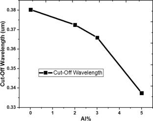
The full electronic band structure of the Al doped ZnO films have been characterized using the TNL-FB™ (full band) simulator from Tech Next Lab. The bandgaps obtained through simulation studies were matched against the experimental bandgap and compared with the results obtained through DFT-based techniques. It was observed that the bandgap value at the Γ-valley increases with the increase in the Al dopant content from 0 at% to 5 at%. The extracted cut-off absorption wavelength was shifted to a shorter wavelength by increasing the Al content, and justifies the Burstein–Moss shift effect. In the present study, the dependency of the topology of the shape of the nanostructure films was taken care of through the lattice disorder effect. The influence of thickness and plane orientation on the various features has been carefully studied. The full electronic band structures of ZnO and AZO samples predicted that the bandgap value is strongly dependent on the internal structure parameter, u. The value of u is significantly affected by lattice disorder generated due to bond angle or length alteration dependent on the topology of the structure and impurity addition. Good agreement was found between the reported and experimental optical bandgap results.
期刊介绍:
The Journal of Electronic Materials (JEM) reports monthly on the science and technology of electronic materials, while examining new applications for semiconductors, magnetic alloys, dielectrics, nanoscale materials, and photonic materials. The journal welcomes articles on methods for preparing and evaluating the chemical, physical, electronic, and optical properties of these materials. Specific areas of interest are materials for state-of-the-art transistors, nanotechnology, electronic packaging, detectors, emitters, metallization, superconductivity, and energy applications.
Review papers on current topics enable individuals in the field of electronics to keep abreast of activities in areas peripheral to their own. JEM also selects papers from conferences such as the Electronic Materials Conference, the U.S. Workshop on the Physics and Chemistry of II-VI Materials, and the International Conference on Thermoelectrics. It benefits both specialists and non-specialists in the electronic materials field.
A journal of The Minerals, Metals & Materials Society.




 京公网安备 11010802042870号
京ICP备2023020795号-1
京公网安备 11010802042870号
京ICP备2023020795号-1

 分享
分享
 求助内容:
求助内容: 应助结果提醒方式:
 扫码关注我们
