Yaqing Shen, Kaichen Zhu, Yiping Xiao, Dominic Waldhör, Abdulrahman H. Basher, Theresia Knobloch, Sebastian Pazos, Xianhu Liang, Wenwen Zheng, Yue Yuan, Juan B. Roldan, Udo Schwingenschlögl, He Tian, Huaqiang Wu, Thomas F. Schranghamer, Nicholas Trainor, Joan M. Redwing, Saptarshi Das, Tibor Grasser, Mario Lanza
{"title":"使用六方氮化硼电介质和高内聚能金属栅极的二维材料晶体管","authors":"Yaqing Shen, Kaichen Zhu, Yiping Xiao, Dominic Waldhör, Abdulrahman H. Basher, Theresia Knobloch, Sebastian Pazos, Xianhu Liang, Wenwen Zheng, Yue Yuan, Juan B. Roldan, Udo Schwingenschlögl, He Tian, Huaqiang Wu, Thomas F. Schranghamer, Nicholas Trainor, Joan M. Redwing, Saptarshi Das, Tibor Grasser, Mario Lanza","doi":"10.1038/s41928-024-01233-w","DOIUrl":null,"url":null,"abstract":"Two-dimensional (2D) semiconductors could potentially be used as channel materials in commercial field-effect transistors. However, the interface between 2D semiconductors and most gate dielectrics contains traps that degrade performance. Layered hexagonal boron nitride (h-BN) can form a defect-free interface with 2D semiconductors, but when prepared by industry-compatible methods—such as chemical vapour deposition (CVD)—the presence of native defects increases leakage current and reduces dielectric strength. Here we show that metal gate electrodes with a high cohesive energy—platinum and tungsten—can allow CVD-grown layered h-BN to be used as a gate dielectric in transistors. The electrodes can reduce the current across CVD-grown h-BN by a factor of around 500 compared to similar devices with gold electrodes and can provide a high dielectric strength of at least 25 MV cm−1. We examine the behaviour statistically across 867 devices, which includes a microchip based on complementary metal–oxide–semiconductor technology. Metal gate electrodes with a high cohesive energy—platinum and tungsten—can be used to mitigate leakage currents and premature dielectric breakdown across chemical vapour deposition-grown multilayer hexagonal boron nitride, allowing the material to be used as a gate dielectric in two-dimensional-materials-based transistors.","PeriodicalId":19064,"journal":{"name":"Nature Electronics","volume":"7 10","pages":"856-867"},"PeriodicalIF":40.9000,"publicationDate":"2024-08-26","publicationTypes":"Journal Article","fieldsOfStudy":null,"isOpenAccess":false,"openAccessPdf":"","citationCount":"0","resultStr":"{\"title\":\"Two-dimensional-materials-based transistors using hexagonal boron nitride dielectrics and metal gate electrodes with high cohesive energy\",\"authors\":\"Yaqing Shen, Kaichen Zhu, Yiping Xiao, Dominic Waldhör, Abdulrahman H. Basher, Theresia Knobloch, Sebastian Pazos, Xianhu Liang, Wenwen Zheng, Yue Yuan, Juan B. Roldan, Udo Schwingenschlögl, He Tian, Huaqiang Wu, Thomas F. Schranghamer, Nicholas Trainor, Joan M. Redwing, Saptarshi Das, Tibor Grasser, Mario Lanza\",\"doi\":\"10.1038/s41928-024-01233-w\",\"DOIUrl\":null,\"url\":null,\"abstract\":\"Two-dimensional (2D) semiconductors could potentially be used as channel materials in commercial field-effect transistors. However, the interface between 2D semiconductors and most gate dielectrics contains traps that degrade performance. Layered hexagonal boron nitride (h-BN) can form a defect-free interface with 2D semiconductors, but when prepared by industry-compatible methods—such as chemical vapour deposition (CVD)—the presence of native defects increases leakage current and reduces dielectric strength. Here we show that metal gate electrodes with a high cohesive energy—platinum and tungsten—can allow CVD-grown layered h-BN to be used as a gate dielectric in transistors. The electrodes can reduce the current across CVD-grown h-BN by a factor of around 500 compared to similar devices with gold electrodes and can provide a high dielectric strength of at least 25 MV cm−1. We examine the behaviour statistically across 867 devices, which includes a microchip based on complementary metal–oxide–semiconductor technology. Metal gate electrodes with a high cohesive energy—platinum and tungsten—can be used to mitigate leakage currents and premature dielectric breakdown across chemical vapour deposition-grown multilayer hexagonal boron nitride, allowing the material to be used as a gate dielectric in two-dimensional-materials-based transistors.\",\"PeriodicalId\":19064,\"journal\":{\"name\":\"Nature Electronics\",\"volume\":\"7 10\",\"pages\":\"856-867\"},\"PeriodicalIF\":40.9000,\"publicationDate\":\"2024-08-26\",\"publicationTypes\":\"Journal Article\",\"fieldsOfStudy\":null,\"isOpenAccess\":false,\"openAccessPdf\":\"\",\"citationCount\":\"0\",\"resultStr\":null,\"platform\":\"Semanticscholar\",\"paperid\":null,\"PeriodicalName\":\"Nature Electronics\",\"FirstCategoryId\":\"5\",\"ListUrlMain\":\"https://www.nature.com/articles/s41928-024-01233-w\",\"RegionNum\":1,\"RegionCategory\":\"工程技术\",\"ArticlePicture\":[],\"TitleCN\":null,\"AbstractTextCN\":null,\"PMCID\":null,\"EPubDate\":\"\",\"PubModel\":\"\",\"JCR\":\"Q1\",\"JCRName\":\"ENGINEERING, ELECTRICAL & ELECTRONIC\",\"Score\":null,\"Total\":0}","platform":"Semanticscholar","paperid":null,"PeriodicalName":"Nature Electronics","FirstCategoryId":"5","ListUrlMain":"https://www.nature.com/articles/s41928-024-01233-w","RegionNum":1,"RegionCategory":"工程技术","ArticlePicture":[],"TitleCN":null,"AbstractTextCN":null,"PMCID":null,"EPubDate":"","PubModel":"","JCR":"Q1","JCRName":"ENGINEERING, ELECTRICAL & ELECTRONIC","Score":null,"Total":0}
Two-dimensional-materials-based transistors using hexagonal boron nitride dielectrics and metal gate electrodes with high cohesive energy
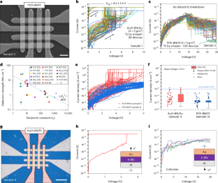
Two-dimensional (2D) semiconductors could potentially be used as channel materials in commercial field-effect transistors. However, the interface between 2D semiconductors and most gate dielectrics contains traps that degrade performance. Layered hexagonal boron nitride (h-BN) can form a defect-free interface with 2D semiconductors, but when prepared by industry-compatible methods—such as chemical vapour deposition (CVD)—the presence of native defects increases leakage current and reduces dielectric strength. Here we show that metal gate electrodes with a high cohesive energy—platinum and tungsten—can allow CVD-grown layered h-BN to be used as a gate dielectric in transistors. The electrodes can reduce the current across CVD-grown h-BN by a factor of around 500 compared to similar devices with gold electrodes and can provide a high dielectric strength of at least 25 MV cm−1. We examine the behaviour statistically across 867 devices, which includes a microchip based on complementary metal–oxide–semiconductor technology. Metal gate electrodes with a high cohesive energy—platinum and tungsten—can be used to mitigate leakage currents and premature dielectric breakdown across chemical vapour deposition-grown multilayer hexagonal boron nitride, allowing the material to be used as a gate dielectric in two-dimensional-materials-based transistors.
期刊介绍:
Nature Electronics is a comprehensive journal that publishes both fundamental and applied research in the field of electronics. It encompasses a wide range of topics, including the study of new phenomena and devices, the design and construction of electronic circuits, and the practical applications of electronics. In addition, the journal explores the commercial and industrial aspects of electronics research.
The primary focus of Nature Electronics is on the development of technology and its potential impact on society. The journal incorporates the contributions of scientists, engineers, and industry professionals, offering a platform for their research findings. Moreover, Nature Electronics provides insightful commentary, thorough reviews, and analysis of the key issues that shape the field, as well as the technologies that are reshaping society.
Like all journals within the prestigious Nature brand, Nature Electronics upholds the highest standards of quality. It maintains a dedicated team of professional editors and follows a fair and rigorous peer-review process. The journal also ensures impeccable copy-editing and production, enabling swift publication. Additionally, Nature Electronics prides itself on its editorial independence, ensuring unbiased and impartial reporting.
In summary, Nature Electronics is a leading journal that publishes cutting-edge research in electronics. With its multidisciplinary approach and commitment to excellence, the journal serves as a valuable resource for scientists, engineers, and industry professionals seeking to stay at the forefront of advancements in the field.


 分享
分享
 求助内容:
求助内容: 应助结果提醒方式:
 扫码关注我们
