Dasari Venkatakrishnarao, Abhishek Mishra, Yaoju Tarn, Michel Bosman, Rainer Lee, Sarthak Das, Subhrajit Mukherjee, Teymour Talha-Dean, Yiyu Zhang, Siew Lang Teo, Jianwei Chai, Fabio Bussolotti, Kuan Eng Johnson Goh, Chit Siong Lau
{"title":"液态金属氧化物辅助集成高 k 电介质和金属触点以实现二维电子器件","authors":"Dasari Venkatakrishnarao, Abhishek Mishra, Yaoju Tarn, Michel Bosman, Rainer Lee, Sarthak Das, Subhrajit Mukherjee, Teymour Talha-Dean, Yiyu Zhang, Siew Lang Teo, Jianwei Chai, Fabio Bussolotti, Kuan Eng Johnson Goh, Chit Siong Lau","doi":"10.1021/acsnano.4c08554","DOIUrl":null,"url":null,"abstract":"Two-dimensional van der Waals semiconductors are promising for future nanoelectronics. However, integrating high-k gate dielectrics for device applications is challenging as the inert van der Waals material surfaces hinder uniform dielectric growth. Here, we report a liquid metal oxide-assisted approach to integrate ultrathin, high-k HfO<sub>2</sub> dielectric on 2D semiconductors with atomically smooth interfaces. Using this approach, we fabricated 2D WS<sub>2</sub> top-gated transistors with subthreshold swings down to 74.5 mV/dec, gate leakage current density below 10<sup>–6</sup> A/cm<sup>2</sup>, and negligible hysteresis. We further demonstrate a one-step van der Waals integration of contacts and dielectrics on graphene. This can offer a scalable approach toward integrating entire prefabricated device stack arrays with 2D materials. Our work provides a scalable solution to address the crucial dielectric engineering challenge for 2D semiconductor-based electronics.","PeriodicalId":21,"journal":{"name":"ACS Nano","volume":"9 1","pages":""},"PeriodicalIF":16.0000,"publicationDate":"2024-09-18","publicationTypes":"Journal Article","fieldsOfStudy":null,"isOpenAccess":false,"openAccessPdf":"","citationCount":"0","resultStr":"{\"title\":\"Liquid Metal Oxide-Assisted Integration of High-k Dielectrics and Metal Contacts for Two-Dimensional Electronics\",\"authors\":\"Dasari Venkatakrishnarao, Abhishek Mishra, Yaoju Tarn, Michel Bosman, Rainer Lee, Sarthak Das, Subhrajit Mukherjee, Teymour Talha-Dean, Yiyu Zhang, Siew Lang Teo, Jianwei Chai, Fabio Bussolotti, Kuan Eng Johnson Goh, Chit Siong Lau\",\"doi\":\"10.1021/acsnano.4c08554\",\"DOIUrl\":null,\"url\":null,\"abstract\":\"Two-dimensional van der Waals semiconductors are promising for future nanoelectronics. However, integrating high-k gate dielectrics for device applications is challenging as the inert van der Waals material surfaces hinder uniform dielectric growth. Here, we report a liquid metal oxide-assisted approach to integrate ultrathin, high-k HfO<sub>2</sub> dielectric on 2D semiconductors with atomically smooth interfaces. Using this approach, we fabricated 2D WS<sub>2</sub> top-gated transistors with subthreshold swings down to 74.5 mV/dec, gate leakage current density below 10<sup>–6</sup> A/cm<sup>2</sup>, and negligible hysteresis. We further demonstrate a one-step van der Waals integration of contacts and dielectrics on graphene. This can offer a scalable approach toward integrating entire prefabricated device stack arrays with 2D materials. Our work provides a scalable solution to address the crucial dielectric engineering challenge for 2D semiconductor-based electronics.\",\"PeriodicalId\":21,\"journal\":{\"name\":\"ACS Nano\",\"volume\":\"9 1\",\"pages\":\"\"},\"PeriodicalIF\":16.0000,\"publicationDate\":\"2024-09-18\",\"publicationTypes\":\"Journal Article\",\"fieldsOfStudy\":null,\"isOpenAccess\":false,\"openAccessPdf\":\"\",\"citationCount\":\"0\",\"resultStr\":null,\"platform\":\"Semanticscholar\",\"paperid\":null,\"PeriodicalName\":\"ACS Nano\",\"FirstCategoryId\":\"88\",\"ListUrlMain\":\"https://doi.org/10.1021/acsnano.4c08554\",\"RegionNum\":1,\"RegionCategory\":\"材料科学\",\"ArticlePicture\":[],\"TitleCN\":null,\"AbstractTextCN\":null,\"PMCID\":null,\"EPubDate\":\"\",\"PubModel\":\"\",\"JCR\":\"Q1\",\"JCRName\":\"CHEMISTRY, MULTIDISCIPLINARY\",\"Score\":null,\"Total\":0}","platform":"Semanticscholar","paperid":null,"PeriodicalName":"ACS Nano","FirstCategoryId":"88","ListUrlMain":"https://doi.org/10.1021/acsnano.4c08554","RegionNum":1,"RegionCategory":"材料科学","ArticlePicture":[],"TitleCN":null,"AbstractTextCN":null,"PMCID":null,"EPubDate":"","PubModel":"","JCR":"Q1","JCRName":"CHEMISTRY, MULTIDISCIPLINARY","Score":null,"Total":0}
Liquid Metal Oxide-Assisted Integration of High-k Dielectrics and Metal Contacts for Two-Dimensional Electronics
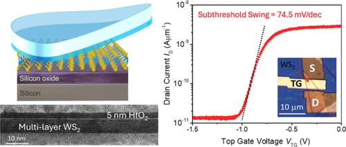
Two-dimensional van der Waals semiconductors are promising for future nanoelectronics. However, integrating high-k gate dielectrics for device applications is challenging as the inert van der Waals material surfaces hinder uniform dielectric growth. Here, we report a liquid metal oxide-assisted approach to integrate ultrathin, high-k HfO2 dielectric on 2D semiconductors with atomically smooth interfaces. Using this approach, we fabricated 2D WS2 top-gated transistors with subthreshold swings down to 74.5 mV/dec, gate leakage current density below 10–6 A/cm2, and negligible hysteresis. We further demonstrate a one-step van der Waals integration of contacts and dielectrics on graphene. This can offer a scalable approach toward integrating entire prefabricated device stack arrays with 2D materials. Our work provides a scalable solution to address the crucial dielectric engineering challenge for 2D semiconductor-based electronics.
期刊介绍:
ACS Nano, published monthly, serves as an international forum for comprehensive articles on nanoscience and nanotechnology research at the intersections of chemistry, biology, materials science, physics, and engineering. The journal fosters communication among scientists in these communities, facilitating collaboration, new research opportunities, and advancements through discoveries. ACS Nano covers synthesis, assembly, characterization, theory, and simulation of nanostructures, nanobiotechnology, nanofabrication, methods and tools for nanoscience and nanotechnology, and self- and directed-assembly. Alongside original research articles, it offers thorough reviews, perspectives on cutting-edge research, and discussions envisioning the future of nanoscience and nanotechnology.


 分享
分享
 求助内容:
求助内容: 应助结果提醒方式:
 扫码关注我们
