Heqing Ye, Hyeok-jin Kwon, Ka Yeon Ryu, Yufei Lu, Hyun Ho Choi, Sang Yong Nam, Zixiao Feng, Jeongwan Park, Jaewon Mo, Hongjian Zhang, Jihoon Lee, Hoyoul Kong and Se Hyun Kim
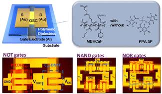
{"title":"通过氟基交联技术提高氟化聚合物绝缘层表面性能,实现高性能有机电子应用†。","authors":"Heqing Ye, Hyeok-jin Kwon, Ka Yeon Ryu, Yufei Lu, Hyun Ho Choi, Sang Yong Nam, Zixiao Feng, Jeongwan Park, Jaewon Mo, Hongjian Zhang, Jihoon Lee, Hoyoul Kong and Se Hyun Kim","doi":"10.1039/D4TC03296A","DOIUrl":null,"url":null,"abstract":"<p >Insulating polymeric layers, like fluorinated polymers, are excellent dielectric materials for organic field-effect transistors (OFETs). However, their high hydrophobicity hinders the deposition of crystalline organic semiconductors, and the poor interface formed deteriorates the charge transfer characteristics. To improve the interface between the dielectric and organic semiconductor, the hydrophobicity of the polymer dielectric must be slightly reduced. Herein, we report the surface tuning of fluorinated dielectrics by the incorporation of fluorine-based UV-assisted crosslinkers. Because the crosslinker is also fluorine-based, the dielectric polymer solution can be homogenously mixed and deposited by a facile printing process to produce a highly polymerized film with excellent insulating properties. Characterization results confirm that the dielectric with crosslinkers enables the formation of an organic semiconductor layer with large crystal grains that facilitates charge transfer at the interface. As the characterization results, transfer curves, and bias-stress test results revealed, the high-quality interface enabled the successful fabrication of OFETs with excellent electrical performance and high thermal stability. The printing process was then applied to integrate multiple n-type and p-type OFETs into NOT, NOR, and NAND gates, demonstrating that the surface modulation of organic dielectrics is scalable and effective in fabricating stable and high-performance large-area organic field-effect devices.</p>","PeriodicalId":84,"journal":{"name":"Journal of Materials Chemistry C","volume":" 42","pages":" 17223-17232"},"PeriodicalIF":5.1000,"publicationDate":"2024-09-24","publicationTypes":"Journal Article","fieldsOfStudy":null,"isOpenAccess":false,"openAccessPdf":"","citationCount":"0","resultStr":"{\"title\":\"Fluorinated polymeric insulating layer surface advancement by fluorine based cross-linking for high-performance organic electronic applications†\",\"authors\":\"Heqing Ye, Hyeok-jin Kwon, Ka Yeon Ryu, Yufei Lu, Hyun Ho Choi, Sang Yong Nam, Zixiao Feng, Jeongwan Park, Jaewon Mo, Hongjian Zhang, Jihoon Lee, Hoyoul Kong and Se Hyun Kim\",\"doi\":\"10.1039/D4TC03296A\",\"DOIUrl\":null,\"url\":null,\"abstract\":\"<p >Insulating polymeric layers, like fluorinated polymers, are excellent dielectric materials for organic field-effect transistors (OFETs). However, their high hydrophobicity hinders the deposition of crystalline organic semiconductors, and the poor interface formed deteriorates the charge transfer characteristics. To improve the interface between the dielectric and organic semiconductor, the hydrophobicity of the polymer dielectric must be slightly reduced. Herein, we report the surface tuning of fluorinated dielectrics by the incorporation of fluorine-based UV-assisted crosslinkers. Because the crosslinker is also fluorine-based, the dielectric polymer solution can be homogenously mixed and deposited by a facile printing process to produce a highly polymerized film with excellent insulating properties. Characterization results confirm that the dielectric with crosslinkers enables the formation of an organic semiconductor layer with large crystal grains that facilitates charge transfer at the interface. As the characterization results, transfer curves, and bias-stress test results revealed, the high-quality interface enabled the successful fabrication of OFETs with excellent electrical performance and high thermal stability. The printing process was then applied to integrate multiple n-type and p-type OFETs into NOT, NOR, and NAND gates, demonstrating that the surface modulation of organic dielectrics is scalable and effective in fabricating stable and high-performance large-area organic field-effect devices.</p>\",\"PeriodicalId\":84,\"journal\":{\"name\":\"Journal of Materials Chemistry C\",\"volume\":\" 42\",\"pages\":\" 17223-17232\"},\"PeriodicalIF\":5.1000,\"publicationDate\":\"2024-09-24\",\"publicationTypes\":\"Journal Article\",\"fieldsOfStudy\":null,\"isOpenAccess\":false,\"openAccessPdf\":\"\",\"citationCount\":\"0\",\"resultStr\":null,\"platform\":\"Semanticscholar\",\"paperid\":null,\"PeriodicalName\":\"Journal of Materials Chemistry C\",\"FirstCategoryId\":\"1\",\"ListUrlMain\":\"https://pubs.rsc.org/en/content/articlelanding/2024/tc/d4tc03296a\",\"RegionNum\":2,\"RegionCategory\":\"材料科学\",\"ArticlePicture\":[],\"TitleCN\":null,\"AbstractTextCN\":null,\"PMCID\":null,\"EPubDate\":\"\",\"PubModel\":\"\",\"JCR\":\"Q2\",\"JCRName\":\"MATERIALS SCIENCE, MULTIDISCIPLINARY\",\"Score\":null,\"Total\":0}","platform":"Semanticscholar","paperid":null,"PeriodicalName":"Journal of Materials Chemistry C","FirstCategoryId":"1","ListUrlMain":"https://pubs.rsc.org/en/content/articlelanding/2024/tc/d4tc03296a","RegionNum":2,"RegionCategory":"材料科学","ArticlePicture":[],"TitleCN":null,"AbstractTextCN":null,"PMCID":null,"EPubDate":"","PubModel":"","JCR":"Q2","JCRName":"MATERIALS SCIENCE, MULTIDISCIPLINARY","Score":null,"Total":0}
引用次数: 0
摘要
绝缘聚合物层(如含氟聚合物)是有机场效应晶体管(OFET)的绝佳介电材料。然而,它们的高疏水性阻碍了晶体有机半导体的沉积,而且形成的不良界面会降低电荷传输特性。为了改善电介质和有机半导体之间的界面,必须稍微降低聚合物电介质的疏水性。在此,我们报告了通过加入氟基紫外线辅助交联剂对含氟电介质进行表面调整的情况。由于交联剂也是氟基的,电介质聚合物溶液可以均匀混合,并通过简便的印刷工艺沉积成具有优异绝缘性能的高聚合薄膜。表征结果证实,含有交联剂的电介质能形成具有大晶粒的有机半导体层,从而促进界面上的电荷转移。表征结果、转移曲线和偏压测试结果表明,高质量的界面能够成功制造出具有优异电气性能和高热稳定性的 OFET。打印工艺随后被用于将多个 n 型和 p 型 OFET 集成到 NOT、NOR 和 NAND 栅极中,证明了有机电介质的表面调制在制造稳定、高性能的大面积有机场效应器件方面具有可扩展性和有效性。
Fluorinated polymeric insulating layer surface advancement by fluorine based cross-linking for high-performance organic electronic applications†
Insulating polymeric layers, like fluorinated polymers, are excellent dielectric materials for organic field-effect transistors (OFETs). However, their high hydrophobicity hinders the deposition of crystalline organic semiconductors, and the poor interface formed deteriorates the charge transfer characteristics. To improve the interface between the dielectric and organic semiconductor, the hydrophobicity of the polymer dielectric must be slightly reduced. Herein, we report the surface tuning of fluorinated dielectrics by the incorporation of fluorine-based UV-assisted crosslinkers. Because the crosslinker is also fluorine-based, the dielectric polymer solution can be homogenously mixed and deposited by a facile printing process to produce a highly polymerized film with excellent insulating properties. Characterization results confirm that the dielectric with crosslinkers enables the formation of an organic semiconductor layer with large crystal grains that facilitates charge transfer at the interface. As the characterization results, transfer curves, and bias-stress test results revealed, the high-quality interface enabled the successful fabrication of OFETs with excellent electrical performance and high thermal stability. The printing process was then applied to integrate multiple n-type and p-type OFETs into NOT, NOR, and NAND gates, demonstrating that the surface modulation of organic dielectrics is scalable and effective in fabricating stable and high-performance large-area organic field-effect devices.
期刊介绍:
The Journal of Materials Chemistry is divided into three distinct sections, A, B, and C, each catering to specific applications of the materials under study:
Journal of Materials Chemistry A focuses primarily on materials intended for applications in energy and sustainability.
Journal of Materials Chemistry B specializes in materials designed for applications in biology and medicine.
Journal of Materials Chemistry C is dedicated to materials suitable for applications in optical, magnetic, and electronic devices.
Example topic areas within the scope of Journal of Materials Chemistry C are listed below. This list is neither exhaustive nor exclusive.
Bioelectronics
Conductors
Detectors
Dielectrics
Displays
Ferroelectrics
Lasers
LEDs
Lighting
Liquid crystals
Memory
Metamaterials
Multiferroics
Photonics
Photovoltaics
Semiconductors
Sensors
Single molecule conductors
Spintronics
Superconductors
Thermoelectrics
Topological insulators
Transistors


 分享
分享
 求助内容:
求助内容: 应助结果提醒方式:
 扫码关注我们
