Li Xu, Haowei Liu, Jianmei Xu, Wei Zhou, Zhihong Yang, Wei Xu, Jian Sun
{"title":"喷雾沉积透明 p 型掺锡铜离子薄膜及其超高速自供电光电探测器。","authors":"Li Xu, Haowei Liu, Jianmei Xu, Wei Zhou, Zhihong Yang, Wei Xu, Jian Sun","doi":"10.1021/acsami.4c11974","DOIUrl":null,"url":null,"abstract":"<p><p>The exploitation of simply processed p-type semiconductors and photodetectors with promising optoelectrical properties remains challenging yet essential for current and future advanced optoelectronic applications. Transparent p-type CuI and Sn-doped CuI (Cu-Sn-I) films and their self-powered photodetectors have been successfully fabricated by the spraying method. It is found that the incorporation of Sn dopants enhances the optical, electrical, and photoelectric properties of CuI thin films as well as their corresponding self-powered heterojunction photodetectors. This improvement of the optoelectrical properties of the Cu-Sn-I film and its photodetector can be attributed to the adjustment of the acceptor defect level and increased hole concentration resulting from Sn doping. The Cu-Sn-I/n-Si photodetector exhibits a responsivity of 10.7 mA/W, a detectivity of 6.79 × 10<sup>11</sup> Jones, and a response time of 77 μs/30 μs (0 V bias). The response time exhibits the fastest rise and decay times compared with the other CuI-based self-powered UV photodetectors in recent years, showcasing promising applications in the realm of transparent electronics moving forward. This study also presents an effective strategy for enhancing the electrical properties of p-type semiconductors and devices through effective doping.</p>","PeriodicalId":5,"journal":{"name":"ACS Applied Materials & Interfaces","volume":" ","pages":"62326-62334"},"PeriodicalIF":7.8000,"publicationDate":"2024-11-13","publicationTypes":"Journal Article","fieldsOfStudy":null,"isOpenAccess":false,"openAccessPdf":"","citationCount":"0","resultStr":"{\"title\":\"Spraying-Deposited Transparent p-Type Sn-Doped CuI Film and Its Ultrahigh-Speed Self-Powered Photodetector.\",\"authors\":\"Li Xu, Haowei Liu, Jianmei Xu, Wei Zhou, Zhihong Yang, Wei Xu, Jian Sun\",\"doi\":\"10.1021/acsami.4c11974\",\"DOIUrl\":null,\"url\":null,\"abstract\":\"<p><p>The exploitation of simply processed p-type semiconductors and photodetectors with promising optoelectrical properties remains challenging yet essential for current and future advanced optoelectronic applications. Transparent p-type CuI and Sn-doped CuI (Cu-Sn-I) films and their self-powered photodetectors have been successfully fabricated by the spraying method. It is found that the incorporation of Sn dopants enhances the optical, electrical, and photoelectric properties of CuI thin films as well as their corresponding self-powered heterojunction photodetectors. This improvement of the optoelectrical properties of the Cu-Sn-I film and its photodetector can be attributed to the adjustment of the acceptor defect level and increased hole concentration resulting from Sn doping. The Cu-Sn-I/n-Si photodetector exhibits a responsivity of 10.7 mA/W, a detectivity of 6.79 × 10<sup>11</sup> Jones, and a response time of 77 μs/30 μs (0 V bias). The response time exhibits the fastest rise and decay times compared with the other CuI-based self-powered UV photodetectors in recent years, showcasing promising applications in the realm of transparent electronics moving forward. This study also presents an effective strategy for enhancing the electrical properties of p-type semiconductors and devices through effective doping.</p>\",\"PeriodicalId\":5,\"journal\":{\"name\":\"ACS Applied Materials & Interfaces\",\"volume\":\" \",\"pages\":\"62326-62334\"},\"PeriodicalIF\":7.8000,\"publicationDate\":\"2024-11-13\",\"publicationTypes\":\"Journal Article\",\"fieldsOfStudy\":null,\"isOpenAccess\":false,\"openAccessPdf\":\"\",\"citationCount\":\"0\",\"resultStr\":null,\"platform\":\"Semanticscholar\",\"paperid\":null,\"PeriodicalName\":\"ACS Applied Materials & Interfaces\",\"FirstCategoryId\":\"88\",\"ListUrlMain\":\"https://doi.org/10.1021/acsami.4c11974\",\"RegionNum\":2,\"RegionCategory\":\"材料科学\",\"ArticlePicture\":[],\"TitleCN\":null,\"AbstractTextCN\":null,\"PMCID\":null,\"EPubDate\":\"2024/11/4 0:00:00\",\"PubModel\":\"Epub\",\"JCR\":\"Q1\",\"JCRName\":\"MATERIALS SCIENCE, MULTIDISCIPLINARY\",\"Score\":null,\"Total\":0}","platform":"Semanticscholar","paperid":null,"PeriodicalName":"ACS Applied Materials & Interfaces","FirstCategoryId":"88","ListUrlMain":"https://doi.org/10.1021/acsami.4c11974","RegionNum":2,"RegionCategory":"材料科学","ArticlePicture":[],"TitleCN":null,"AbstractTextCN":null,"PMCID":null,"EPubDate":"2024/11/4 0:00:00","PubModel":"Epub","JCR":"Q1","JCRName":"MATERIALS SCIENCE, MULTIDISCIPLINARY","Score":null,"Total":0}
引用次数: 0
摘要
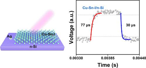
开发具有良好光电特性的简单加工 p 型半导体和光电探测器仍然具有挑战性,但对于当前和未来的先进光电应用至关重要。通过喷涂方法,我们成功地制造出了透明的 p 型 CuI 和 Sn 掺杂 CuI(Cu-Sn-I)薄膜及其自供电光电探测器。研究发现,锡掺杂物的加入增强了 CuI 薄膜及其相应的自供电异质结光电探测器的光学、电学和光电特性。Cu-Sn-I 薄膜及其光电探测器光电特性的改善可归因于掺杂锡后受体缺陷水平的调整和空穴浓度的增加。Cu-Sn-I/n-Si 光电探测器的响应率为 10.7 mA/W,探测率为 6.79 × 10¹¹ Jones,响应时间为 77 μs/30μs(0 V 偏置)。与近年来其他基于 CuI 的自供电紫外光检测器相比,其响应时间具有最快的上升和衰减时间,在透明电子学领域的应用前景十分广阔。这项研究还提出了一种通过有效掺杂来增强 p 型半导体和器件电气性能的有效策略。
Spraying-Deposited Transparent p-Type Sn-Doped CuI Film and Its Ultrahigh-Speed Self-Powered Photodetector.
The exploitation of simply processed p-type semiconductors and photodetectors with promising optoelectrical properties remains challenging yet essential for current and future advanced optoelectronic applications. Transparent p-type CuI and Sn-doped CuI (Cu-Sn-I) films and their self-powered photodetectors have been successfully fabricated by the spraying method. It is found that the incorporation of Sn dopants enhances the optical, electrical, and photoelectric properties of CuI thin films as well as their corresponding self-powered heterojunction photodetectors. This improvement of the optoelectrical properties of the Cu-Sn-I film and its photodetector can be attributed to the adjustment of the acceptor defect level and increased hole concentration resulting from Sn doping. The Cu-Sn-I/n-Si photodetector exhibits a responsivity of 10.7 mA/W, a detectivity of 6.79 × 10¹¹ Jones, and a response time of 77 μs/30 μs (0 V bias). The response time exhibits the fastest rise and decay times compared with the other CuI-based self-powered UV photodetectors in recent years, showcasing promising applications in the realm of transparent electronics moving forward. This study also presents an effective strategy for enhancing the electrical properties of p-type semiconductors and devices through effective doping.
期刊介绍:
ACS Applied Materials & Interfaces is a leading interdisciplinary journal that brings together chemists, engineers, physicists, and biologists to explore the development and utilization of newly-discovered materials and interfacial processes for specific applications. Our journal has experienced remarkable growth since its establishment in 2009, both in terms of the number of articles published and the impact of the research showcased. We are proud to foster a truly global community, with the majority of published articles originating from outside the United States, reflecting the rapid growth of applied research worldwide.




 京公网安备 11010802042870号
京ICP备2023020795号-1
京公网安备 11010802042870号
京ICP备2023020795号-1

 分享
分享
 求助内容:
求助内容: 应助结果提醒方式:
 扫码关注我们
