Aybuke Tavasli , Leszek A. Majewski , M. Afsar Uddin , Berta Gómez-Lor , Levent Trabzon , Sheida Faraji
{"title":"用于未来OFET应用的zro2 -混合纳米复合MIM电容器的设计及其表征","authors":"Aybuke Tavasli , Leszek A. Majewski , M. Afsar Uddin , Berta Gómez-Lor , Levent Trabzon , Sheida Faraji","doi":"10.1016/j.mssp.2024.109180","DOIUrl":null,"url":null,"abstract":"<div><div>Organic field-effect transistors (OFETs) have been exploited as sensors for a variety of applications due to their excellent advantages over diodes and other electronic devices. Capacitors are one of the key components of the OFET designs that consist of a dielectric layer sandwiched between two parallel metal plates. The dielectric layer should be thin and/or have a high <em>k</em> constant value to achieve a high capacitance value (C<sub>i</sub>, areal capacitance), so more charge carriers can be accumulated at the interface between the dielectric and the organic semiconductor, for OFETs to operate under low voltage (< 3 V). In this study, high-<em>k</em> nanocomposites (NCs) of ZrO<sub>2</sub> metal oxide ceramic nanoparticles (NPs) in varying concentrations blended in two different polymer matrixes, poly(vinylidene fluoride-co-hexafluoropropylene) (PVDF-HFP) and cyanoethyl cellulose (CEC) have been utilised as the dielectric layer in metal-insulator-metal (MIM) capacitors. The physical and electrical properties of fabricated MIM capacitors were evaluated. The measured areal capacitance, <em>C</em><sub><em>i</em></sub>, values demonstrated a gradual rise with increasing ZrO<sub>2</sub> metal oxide content in both polymer matrixes. ZrO<sub>2</sub>-PVDF-HFP-based capacitors exhibited a two-fold increase in <em>C</em><sub><em>i</em></sub>, 91.86 ± 6.1 nF/cm<sup>2</sup> (a 140 % increase) for 10 wt % NP content. Similarly, areal capacitance values of 76 ± 3.03 nF/cm<sup>2</sup> (a 45 % rise) was measured on MIMs using CZ10 dielectric layer. High average dielectric constant (<em>k</em>) values of 28.61 and 35.68 for CZ5 and PZ5, respectively) were obtained. As expected, leakage current density increased for higher NP % in polymer matrixes. Nevertheless, all MIMs yielded average leakage current density < 1.75 × 10<sup>−6</sup> (A/cm<sup>2</sup>) at 2 V. Therefore, the reported nanocomposites are suitable dielectric layers for OFETs and as platforms for gas, chemical and photoactivated sensing devices.</div></div>","PeriodicalId":18240,"journal":{"name":"Materials Science in Semiconductor Processing","volume":"188 ","pages":"Article 109180"},"PeriodicalIF":4.6000,"publicationDate":"2025-03-15","publicationTypes":"Journal Article","fieldsOfStudy":null,"isOpenAccess":false,"openAccessPdf":"","citationCount":"0","resultStr":"{\"title\":\"Designing ZrO2-blended nanocomposite MIM capacitors for future OFET applications and their characterizations\",\"authors\":\"Aybuke Tavasli , Leszek A. Majewski , M. Afsar Uddin , Berta Gómez-Lor , Levent Trabzon , Sheida Faraji\",\"doi\":\"10.1016/j.mssp.2024.109180\",\"DOIUrl\":null,\"url\":null,\"abstract\":\"<div><div>Organic field-effect transistors (OFETs) have been exploited as sensors for a variety of applications due to their excellent advantages over diodes and other electronic devices. Capacitors are one of the key components of the OFET designs that consist of a dielectric layer sandwiched between two parallel metal plates. The dielectric layer should be thin and/or have a high <em>k</em> constant value to achieve a high capacitance value (C<sub>i</sub>, areal capacitance), so more charge carriers can be accumulated at the interface between the dielectric and the organic semiconductor, for OFETs to operate under low voltage (< 3 V). In this study, high-<em>k</em> nanocomposites (NCs) of ZrO<sub>2</sub> metal oxide ceramic nanoparticles (NPs) in varying concentrations blended in two different polymer matrixes, poly(vinylidene fluoride-co-hexafluoropropylene) (PVDF-HFP) and cyanoethyl cellulose (CEC) have been utilised as the dielectric layer in metal-insulator-metal (MIM) capacitors. The physical and electrical properties of fabricated MIM capacitors were evaluated. The measured areal capacitance, <em>C</em><sub><em>i</em></sub>, values demonstrated a gradual rise with increasing ZrO<sub>2</sub> metal oxide content in both polymer matrixes. ZrO<sub>2</sub>-PVDF-HFP-based capacitors exhibited a two-fold increase in <em>C</em><sub><em>i</em></sub>, 91.86 ± 6.1 nF/cm<sup>2</sup> (a 140 % increase) for 10 wt % NP content. Similarly, areal capacitance values of 76 ± 3.03 nF/cm<sup>2</sup> (a 45 % rise) was measured on MIMs using CZ10 dielectric layer. High average dielectric constant (<em>k</em>) values of 28.61 and 35.68 for CZ5 and PZ5, respectively) were obtained. As expected, leakage current density increased for higher NP % in polymer matrixes. Nevertheless, all MIMs yielded average leakage current density < 1.75 × 10<sup>−6</sup> (A/cm<sup>2</sup>) at 2 V. Therefore, the reported nanocomposites are suitable dielectric layers for OFETs and as platforms for gas, chemical and photoactivated sensing devices.</div></div>\",\"PeriodicalId\":18240,\"journal\":{\"name\":\"Materials Science in Semiconductor Processing\",\"volume\":\"188 \",\"pages\":\"Article 109180\"},\"PeriodicalIF\":4.6000,\"publicationDate\":\"2025-03-15\",\"publicationTypes\":\"Journal Article\",\"fieldsOfStudy\":null,\"isOpenAccess\":false,\"openAccessPdf\":\"\",\"citationCount\":\"0\",\"resultStr\":null,\"platform\":\"Semanticscholar\",\"paperid\":null,\"PeriodicalName\":\"Materials Science in Semiconductor Processing\",\"FirstCategoryId\":\"5\",\"ListUrlMain\":\"https://www.sciencedirect.com/science/article/pii/S136980012401076X\",\"RegionNum\":3,\"RegionCategory\":\"工程技术\",\"ArticlePicture\":[],\"TitleCN\":null,\"AbstractTextCN\":null,\"PMCID\":null,\"EPubDate\":\"2024/11/30 0:00:00\",\"PubModel\":\"Epub\",\"JCR\":\"Q2\",\"JCRName\":\"ENGINEERING, ELECTRICAL & ELECTRONIC\",\"Score\":null,\"Total\":0}","platform":"Semanticscholar","paperid":null,"PeriodicalName":"Materials Science in Semiconductor Processing","FirstCategoryId":"5","ListUrlMain":"https://www.sciencedirect.com/science/article/pii/S136980012401076X","RegionNum":3,"RegionCategory":"工程技术","ArticlePicture":[],"TitleCN":null,"AbstractTextCN":null,"PMCID":null,"EPubDate":"2024/11/30 0:00:00","PubModel":"Epub","JCR":"Q2","JCRName":"ENGINEERING, ELECTRICAL & ELECTRONIC","Score":null,"Total":0}
Designing ZrO2-blended nanocomposite MIM capacitors for future OFET applications and their characterizations
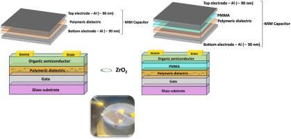
Organic field-effect transistors (OFETs) have been exploited as sensors for a variety of applications due to their excellent advantages over diodes and other electronic devices. Capacitors are one of the key components of the OFET designs that consist of a dielectric layer sandwiched between two parallel metal plates. The dielectric layer should be thin and/or have a high k constant value to achieve a high capacitance value (Ci, areal capacitance), so more charge carriers can be accumulated at the interface between the dielectric and the organic semiconductor, for OFETs to operate under low voltage (< 3 V). In this study, high-k nanocomposites (NCs) of ZrO2 metal oxide ceramic nanoparticles (NPs) in varying concentrations blended in two different polymer matrixes, poly(vinylidene fluoride-co-hexafluoropropylene) (PVDF-HFP) and cyanoethyl cellulose (CEC) have been utilised as the dielectric layer in metal-insulator-metal (MIM) capacitors. The physical and electrical properties of fabricated MIM capacitors were evaluated. The measured areal capacitance, Ci, values demonstrated a gradual rise with increasing ZrO2 metal oxide content in both polymer matrixes. ZrO2-PVDF-HFP-based capacitors exhibited a two-fold increase in Ci, 91.86 ± 6.1 nF/cm2 (a 140 % increase) for 10 wt % NP content. Similarly, areal capacitance values of 76 ± 3.03 nF/cm2 (a 45 % rise) was measured on MIMs using CZ10 dielectric layer. High average dielectric constant (k) values of 28.61 and 35.68 for CZ5 and PZ5, respectively) were obtained. As expected, leakage current density increased for higher NP % in polymer matrixes. Nevertheless, all MIMs yielded average leakage current density < 1.75 × 10⁻⁶ (A/cm2) at 2 V. Therefore, the reported nanocomposites are suitable dielectric layers for OFETs and as platforms for gas, chemical and photoactivated sensing devices.
期刊介绍:
Materials Science in Semiconductor Processing provides a unique forum for the discussion of novel processing, applications and theoretical studies of functional materials and devices for (opto)electronics, sensors, detectors, biotechnology and green energy.
Each issue will aim to provide a snapshot of current insights, new achievements, breakthroughs and future trends in such diverse fields as microelectronics, energy conversion and storage, communications, biotechnology, (photo)catalysis, nano- and thin-film technology, hybrid and composite materials, chemical processing, vapor-phase deposition, device fabrication, and modelling, which are the backbone of advanced semiconductor processing and applications.
Coverage will include: advanced lithography for submicron devices; etching and related topics; ion implantation; damage evolution and related issues; plasma and thermal CVD; rapid thermal processing; advanced metallization and interconnect schemes; thin dielectric layers, oxidation; sol-gel processing; chemical bath and (electro)chemical deposition; compound semiconductor processing; new non-oxide materials and their applications; (macro)molecular and hybrid materials; molecular dynamics, ab-initio methods, Monte Carlo, etc.; new materials and processes for discrete and integrated circuits; magnetic materials and spintronics; heterostructures and quantum devices; engineering of the electrical and optical properties of semiconductors; crystal growth mechanisms; reliability, defect density, intrinsic impurities and defects.




 京公网安备 11010802042870号
京ICP备2023020795号-1
京公网安备 11010802042870号
京ICP备2023020795号-1

 分享
分享
 求助内容:
求助内容: 应助结果提醒方式:
 扫码关注我们
