{"title":"用于快速响应光电探测器的WS2/石墨烯/MoS2夹层范德华异质结","authors":"Yongzhi Zhang, Xunjun He","doi":"10.1021/acsami.4c13818","DOIUrl":null,"url":null,"abstract":"Fast-response photodetectors have attracted considerable attention in the application of high-speed communication, real-time monitoring, and optical imaging systems. However, most reported photodetectors suffer from limitations of the inherent properties of materials, low carrier transport efficiency, and unmatched interfaces, which lead to a low response speed. Here, we report a WS<sub>2</sub>/graphene/MoS<sub>2</sub> vertical van der Waals heterojunction fabricated by mechanical exfoliation and dry transfer methods for fast response. To improve the response speed of the previously reported WS<sub>2</sub>/MoS<sub>2</sub> heterojunction with excellent photoelectric performances, the embedded graphene is employed to optimize the interface defects and improve the carrier transport efficiency due to its high mobility and smooth and flat surface. Under the illuminations of a 405 nm laser and a bias voltage of 0.5 V, our device can realize rise and fall times of 44 and 52 μs, respectively. For a bias voltage of 2.5 V, moreover, the device can also show outstanding performances including a high responsivity of 220 A/W, a considerable detectivity of 1.2 × 10<sup>13</sup> Jones, a large external quantum efficiency of 6.7 × 10<sup>4</sup> %, and a low dark current of 1.05 × 10<sup>–13</sup> A. Additionally, the device enables high-speed transmission with a low bit error rate in a closed-loop optical communication system. Therefore, the proposed scheme can provide an idea for the design of photodetectors with fast response and high performance.","PeriodicalId":5,"journal":{"name":"ACS Applied Materials & Interfaces","volume":"13 1","pages":""},"PeriodicalIF":8.2000,"publicationDate":"2024-12-19","publicationTypes":"Journal Article","fieldsOfStudy":null,"isOpenAccess":false,"openAccessPdf":"","citationCount":"0","resultStr":"{\"title\":\"WS2/Graphene/MoS2 Sandwich van der Waals Heterojunction for Fast-Response Photodetectors\",\"authors\":\"Yongzhi Zhang, Xunjun He\",\"doi\":\"10.1021/acsami.4c13818\",\"DOIUrl\":null,\"url\":null,\"abstract\":\"Fast-response photodetectors have attracted considerable attention in the application of high-speed communication, real-time monitoring, and optical imaging systems. However, most reported photodetectors suffer from limitations of the inherent properties of materials, low carrier transport efficiency, and unmatched interfaces, which lead to a low response speed. Here, we report a WS<sub>2</sub>/graphene/MoS<sub>2</sub> vertical van der Waals heterojunction fabricated by mechanical exfoliation and dry transfer methods for fast response. To improve the response speed of the previously reported WS<sub>2</sub>/MoS<sub>2</sub> heterojunction with excellent photoelectric performances, the embedded graphene is employed to optimize the interface defects and improve the carrier transport efficiency due to its high mobility and smooth and flat surface. Under the illuminations of a 405 nm laser and a bias voltage of 0.5 V, our device can realize rise and fall times of 44 and 52 μs, respectively. For a bias voltage of 2.5 V, moreover, the device can also show outstanding performances including a high responsivity of 220 A/W, a considerable detectivity of 1.2 × 10<sup>13</sup> Jones, a large external quantum efficiency of 6.7 × 10<sup>4</sup> %, and a low dark current of 1.05 × 10<sup>–13</sup> A. Additionally, the device enables high-speed transmission with a low bit error rate in a closed-loop optical communication system. Therefore, the proposed scheme can provide an idea for the design of photodetectors with fast response and high performance.\",\"PeriodicalId\":5,\"journal\":{\"name\":\"ACS Applied Materials & Interfaces\",\"volume\":\"13 1\",\"pages\":\"\"},\"PeriodicalIF\":8.2000,\"publicationDate\":\"2024-12-19\",\"publicationTypes\":\"Journal Article\",\"fieldsOfStudy\":null,\"isOpenAccess\":false,\"openAccessPdf\":\"\",\"citationCount\":\"0\",\"resultStr\":null,\"platform\":\"Semanticscholar\",\"paperid\":null,\"PeriodicalName\":\"ACS Applied Materials & Interfaces\",\"FirstCategoryId\":\"88\",\"ListUrlMain\":\"https://doi.org/10.1021/acsami.4c13818\",\"RegionNum\":2,\"RegionCategory\":\"材料科学\",\"ArticlePicture\":[],\"TitleCN\":null,\"AbstractTextCN\":null,\"PMCID\":null,\"EPubDate\":\"\",\"PubModel\":\"\",\"JCR\":\"Q1\",\"JCRName\":\"MATERIALS SCIENCE, MULTIDISCIPLINARY\",\"Score\":null,\"Total\":0}","platform":"Semanticscholar","paperid":null,"PeriodicalName":"ACS Applied Materials & Interfaces","FirstCategoryId":"88","ListUrlMain":"https://doi.org/10.1021/acsami.4c13818","RegionNum":2,"RegionCategory":"材料科学","ArticlePicture":[],"TitleCN":null,"AbstractTextCN":null,"PMCID":null,"EPubDate":"","PubModel":"","JCR":"Q1","JCRName":"MATERIALS SCIENCE, MULTIDISCIPLINARY","Score":null,"Total":0}
引用次数: 0
摘要
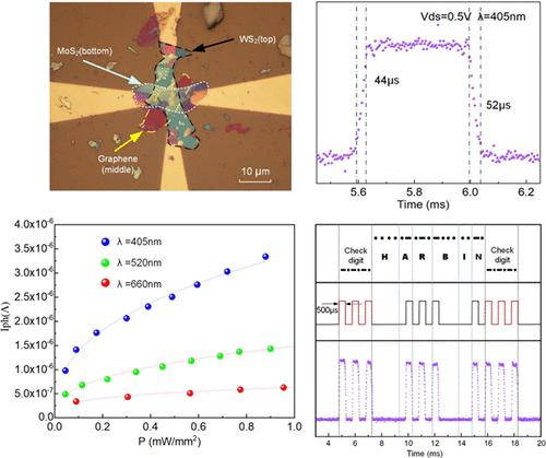
快速响应光电探测器在高速通信、实时监控和光学成像系统的应用中备受关注。然而,大多数已报道的光电探测器都受到材料固有特性、载流子传输效率低和接口不匹配等因素的限制,导致响应速度较低。在此,我们报告了一种通过机械剥离和干法转移方法制造的 WS2/石墨烯/MoS2 垂直范德华异质结,可实现快速响应。为了提高之前报道的具有优异光电性能的 WS2/MoS2 异质结的响应速度,我们采用了嵌入式石墨烯来优化界面缺陷,并利用其高迁移率和光滑平整的表面提高载流子传输效率。在波长为 405 nm 的激光和 0.5 V 的偏置电压照射下,我们的器件可以实现分别为 44 和 52 μs 的上升和下降时间。此外,在偏置电压为 2.5 V 时,该器件还能表现出卓越的性能,包括 220 A/W 的高响应率、1.2 × 10¹³ Jones 的高检测率、6.7 × 10⁴ % 的高外部量子效率以及 1.05 × 10⁻¹³ A 的低暗电流。此外,该器件还能在闭环光通信系统中实现低误码率的高速传输。因此,所提出的方案可以为设计具有快速响应和高性能的光电探测器提供一种思路。
WS2/Graphene/MoS2 Sandwich van der Waals Heterojunction for Fast-Response Photodetectors
Fast-response photodetectors have attracted considerable attention in the application of high-speed communication, real-time monitoring, and optical imaging systems. However, most reported photodetectors suffer from limitations of the inherent properties of materials, low carrier transport efficiency, and unmatched interfaces, which lead to a low response speed. Here, we report a WS2/graphene/MoS2 vertical van der Waals heterojunction fabricated by mechanical exfoliation and dry transfer methods for fast response. To improve the response speed of the previously reported WS2/MoS2 heterojunction with excellent photoelectric performances, the embedded graphene is employed to optimize the interface defects and improve the carrier transport efficiency due to its high mobility and smooth and flat surface. Under the illuminations of a 405 nm laser and a bias voltage of 0.5 V, our device can realize rise and fall times of 44 and 52 μs, respectively. For a bias voltage of 2.5 V, moreover, the device can also show outstanding performances including a high responsivity of 220 A/W, a considerable detectivity of 1.2 × 10¹³ Jones, a large external quantum efficiency of 6.7 × 10⁴ %, and a low dark current of 1.05 × 10⁻¹³ A. Additionally, the device enables high-speed transmission with a low bit error rate in a closed-loop optical communication system. Therefore, the proposed scheme can provide an idea for the design of photodetectors with fast response and high performance.
期刊介绍:
ACS Applied Materials & Interfaces is a leading interdisciplinary journal that brings together chemists, engineers, physicists, and biologists to explore the development and utilization of newly-discovered materials and interfacial processes for specific applications. Our journal has experienced remarkable growth since its establishment in 2009, both in terms of the number of articles published and the impact of the research showcased. We are proud to foster a truly global community, with the majority of published articles originating from outside the United States, reflecting the rapid growth of applied research worldwide.


 分享
分享
 求助内容:
求助内容: 应助结果提醒方式:
 扫码关注我们
