U Jeong Yang, Sehyun Park, Woosung Choi, Vladimir V. Tsukruk
{"title":"金属氧化物纳米颗粒带隙工程微雕刻紫外敏感薄膜晶体管","authors":"U Jeong Yang, Sehyun Park, Woosung Choi, Vladimir V. Tsukruk","doi":"10.1002/aelm.202400798","DOIUrl":null,"url":null,"abstract":"<p>As known, n-type inorganic semiconductor nanoparticles such as zinc oxide nanoparticles have been explored in various sensing applications, which demand high-density electronic elements placement for rapid operation. Herein, high-resolution designs of conductive channels of noble metal-doped zinc oxide nanoparticles is demonstrated using an engraving transfer printing process and silver metal doping approach. Such thin-film transistors with reduced feature size to 2 µm fabricated exhibited significantly enhanced electron mobility up 3.46 × 10<sup>−2</sup> cm<sup>2</sup> V<sup>−1</sup> s<sup>−1</sup> and light sensitivity. Furthermore, the integration of this micropatterning technology and metal doping in thin-film transistors is utilized for control of current–voltage characteristics under the ultraviolet radiation with high sensitivity. It is suggested that this approach to design of doped inorganic nanoparticle channels paves the way for high-density thin-film transistors suitable for optoelectronic circuit, UV photodetectors and neuromorphic computing systems.</p>","PeriodicalId":110,"journal":{"name":"Advanced Electronic Materials","volume":"11 9","pages":""},"PeriodicalIF":5.9000,"publicationDate":"2025-06-17","publicationTypes":"Journal Article","fieldsOfStudy":null,"isOpenAccess":false,"openAccessPdf":"https://onlinelibrary.wiley.com/doi/epdf/10.1002/aelm.202400798","citationCount":"0","resultStr":"{\"title\":\"Micro-Engraving UV-Sensitive Thin-Film Transistor from Metal–Metal Oxide Nanoparticles with Band-Gap Engineering\",\"authors\":\"U Jeong Yang, Sehyun Park, Woosung Choi, Vladimir V. Tsukruk\",\"doi\":\"10.1002/aelm.202400798\",\"DOIUrl\":null,\"url\":null,\"abstract\":\"<p>As known, n-type inorganic semiconductor nanoparticles such as zinc oxide nanoparticles have been explored in various sensing applications, which demand high-density electronic elements placement for rapid operation. Herein, high-resolution designs of conductive channels of noble metal-doped zinc oxide nanoparticles is demonstrated using an engraving transfer printing process and silver metal doping approach. Such thin-film transistors with reduced feature size to 2 µm fabricated exhibited significantly enhanced electron mobility up 3.46 × 10<sup>−2</sup> cm<sup>2</sup> V<sup>−1</sup> s<sup>−1</sup> and light sensitivity. Furthermore, the integration of this micropatterning technology and metal doping in thin-film transistors is utilized for control of current–voltage characteristics under the ultraviolet radiation with high sensitivity. It is suggested that this approach to design of doped inorganic nanoparticle channels paves the way for high-density thin-film transistors suitable for optoelectronic circuit, UV photodetectors and neuromorphic computing systems.</p>\",\"PeriodicalId\":110,\"journal\":{\"name\":\"Advanced Electronic Materials\",\"volume\":\"11 9\",\"pages\":\"\"},\"PeriodicalIF\":5.9000,\"publicationDate\":\"2025-06-17\",\"publicationTypes\":\"Journal Article\",\"fieldsOfStudy\":null,\"isOpenAccess\":false,\"openAccessPdf\":\"https://onlinelibrary.wiley.com/doi/epdf/10.1002/aelm.202400798\",\"citationCount\":\"0\",\"resultStr\":null,\"platform\":\"Semanticscholar\",\"paperid\":null,\"PeriodicalName\":\"Advanced Electronic Materials\",\"FirstCategoryId\":\"88\",\"ListUrlMain\":\"https://onlinelibrary.wiley.com/doi/10.1002/aelm.202400798\",\"RegionNum\":2,\"RegionCategory\":\"材料科学\",\"ArticlePicture\":[],\"TitleCN\":null,\"AbstractTextCN\":null,\"PMCID\":null,\"EPubDate\":\"2025/2/2 0:00:00\",\"PubModel\":\"Epub\",\"JCR\":\"Q2\",\"JCRName\":\"MATERIALS SCIENCE, MULTIDISCIPLINARY\",\"Score\":null,\"Total\":0}","platform":"Semanticscholar","paperid":null,"PeriodicalName":"Advanced Electronic Materials","FirstCategoryId":"88","ListUrlMain":"https://onlinelibrary.wiley.com/doi/10.1002/aelm.202400798","RegionNum":2,"RegionCategory":"材料科学","ArticlePicture":[],"TitleCN":null,"AbstractTextCN":null,"PMCID":null,"EPubDate":"2025/2/2 0:00:00","PubModel":"Epub","JCR":"Q2","JCRName":"MATERIALS SCIENCE, MULTIDISCIPLINARY","Score":null,"Total":0}
Micro-Engraving UV-Sensitive Thin-Film Transistor from Metal–Metal Oxide Nanoparticles with Band-Gap Engineering
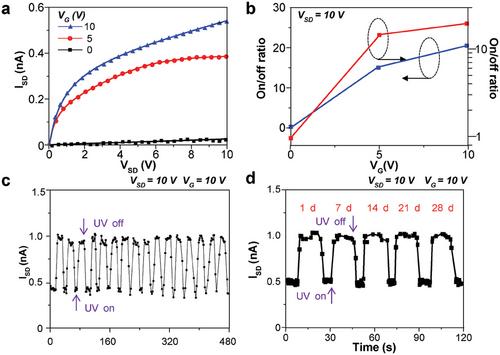
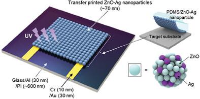
As known, n-type inorganic semiconductor nanoparticles such as zinc oxide nanoparticles have been explored in various sensing applications, which demand high-density electronic elements placement for rapid operation. Herein, high-resolution designs of conductive channels of noble metal-doped zinc oxide nanoparticles is demonstrated using an engraving transfer printing process and silver metal doping approach. Such thin-film transistors with reduced feature size to 2 µm fabricated exhibited significantly enhanced electron mobility up 3.46 × 10⁻² cm2 V−1 s−1 and light sensitivity. Furthermore, the integration of this micropatterning technology and metal doping in thin-film transistors is utilized for control of current–voltage characteristics under the ultraviolet radiation with high sensitivity. It is suggested that this approach to design of doped inorganic nanoparticle channels paves the way for high-density thin-film transistors suitable for optoelectronic circuit, UV photodetectors and neuromorphic computing systems.
期刊介绍:
Advanced Electronic Materials is an interdisciplinary forum for peer-reviewed, high-quality, high-impact research in the fields of materials science, physics, and engineering of electronic and magnetic materials. It includes research on physics and physical properties of electronic and magnetic materials, spintronics, electronics, device physics and engineering, micro- and nano-electromechanical systems, and organic electronics, in addition to fundamental research.







 京公网安备 11010802042870号
京ICP备2023020795号-1
京公网安备 11010802042870号
京ICP备2023020795号-1

 分享
分享
 求助内容:
求助内容: 应助结果提醒方式:
 扫码关注我们
