Abdelmajid Salhi*, Anas Abutaha, Atef Zekri, Mujaheed Pasha, Ayman Samara and Said Mansour,
{"title":"分子束外延在Si(100)上生长高迁移率γ-相硒化铟","authors":"Abdelmajid Salhi*, Anas Abutaha, Atef Zekri, Mujaheed Pasha, Ayman Samara and Said Mansour, ","doi":"10.1021/acsaelm.4c01800","DOIUrl":null,"url":null,"abstract":"<p >III–VI compounds, such as In<sub><i>x</i></sub>Se<sub><i>y</i></sub> materials, offer an unprecedented potential for electronic devices at the atomic level. Despite their superior electronic properties, most research focused on measuring transport locally within mechanically exfoliated flakes at microscale and sometimes transferred on atomically flat surfaces. However, from a technological perspective, the integration of these materials in electronic devices requires wafer-scale, uniformly grown films, preferably integrated with the dominant semiconductor, silicon. Indium selenide films have recently shown promising electronic performance. Unfortunately, the epitaxial growth of single-phase indium selenide poses challenges due to its polymorphic nature and different stoichiometries, such as α-In<sub>2</sub>Se<sub>3</sub>, ε-for InSe, and β, γ for both InSe and In<sub>2</sub>Se<sub>3</sub>. Here, we report the growth of single phase γ-In<sub>2</sub>Se<sub>3</sub> on Si (100), with a Hall mobility exceeding 2000 cm<sup>2</sup>/(V s) at room temperature. Our study explores the growth parameter space in the Molecular Beam Epitaxy (MBE), specifically the Se/In flux ratio and the growth temperature. It correlates them with the structural, morphological, and electrical characteristics of In<sub><i>x</i></sub>Se<sub><i>y</i></sub> films. A phase map was constructed within the specified growth temperature and Se/In flux ranges. γ-In<sub>2</sub>Se<sub>3</sub> single phase formation occurs only in a small temperature and Se/In Flux ratio window. In contrast, the formation of a mixture of γ-InSe and γ-In<sub>2</sub>Se<sub>3</sub> phases is obtained in a large growth condition window. The sensitivity of indium selenide’s electrical and morphological properties to growth conditions implies the necessity for precise adjustments of the Se/In flux ratio alongside the growth temperature to selectively grow large-area single-phase γ-In<sub>2</sub>Se<sub>3</sub> suitable for advanced electronic devices such as field effect transistors and photodetectors.</p>","PeriodicalId":3,"journal":{"name":"ACS Applied Electronic Materials","volume":"7 4","pages":"1398–1407 1398–1407"},"PeriodicalIF":4.7000,"publicationDate":"2025-02-15","publicationTypes":"Journal Article","fieldsOfStudy":null,"isOpenAccess":false,"openAccessPdf":"","citationCount":"0","resultStr":"{\"title\":\"High Mobility γ-Phase Indium Selenide on Si(100) Grown by Molecular Beam Epitaxy\",\"authors\":\"Abdelmajid Salhi*, Anas Abutaha, Atef Zekri, Mujaheed Pasha, Ayman Samara and Said Mansour, \",\"doi\":\"10.1021/acsaelm.4c01800\",\"DOIUrl\":null,\"url\":null,\"abstract\":\"<p >III–VI compounds, such as In<sub><i>x</i></sub>Se<sub><i>y</i></sub> materials, offer an unprecedented potential for electronic devices at the atomic level. Despite their superior electronic properties, most research focused on measuring transport locally within mechanically exfoliated flakes at microscale and sometimes transferred on atomically flat surfaces. However, from a technological perspective, the integration of these materials in electronic devices requires wafer-scale, uniformly grown films, preferably integrated with the dominant semiconductor, silicon. Indium selenide films have recently shown promising electronic performance. Unfortunately, the epitaxial growth of single-phase indium selenide poses challenges due to its polymorphic nature and different stoichiometries, such as α-In<sub>2</sub>Se<sub>3</sub>, ε-for InSe, and β, γ for both InSe and In<sub>2</sub>Se<sub>3</sub>. Here, we report the growth of single phase γ-In<sub>2</sub>Se<sub>3</sub> on Si (100), with a Hall mobility exceeding 2000 cm<sup>2</sup>/(V s) at room temperature. Our study explores the growth parameter space in the Molecular Beam Epitaxy (MBE), specifically the Se/In flux ratio and the growth temperature. It correlates them with the structural, morphological, and electrical characteristics of In<sub><i>x</i></sub>Se<sub><i>y</i></sub> films. A phase map was constructed within the specified growth temperature and Se/In flux ranges. γ-In<sub>2</sub>Se<sub>3</sub> single phase formation occurs only in a small temperature and Se/In Flux ratio window. In contrast, the formation of a mixture of γ-InSe and γ-In<sub>2</sub>Se<sub>3</sub> phases is obtained in a large growth condition window. The sensitivity of indium selenide’s electrical and morphological properties to growth conditions implies the necessity for precise adjustments of the Se/In flux ratio alongside the growth temperature to selectively grow large-area single-phase γ-In<sub>2</sub>Se<sub>3</sub> suitable for advanced electronic devices such as field effect transistors and photodetectors.</p>\",\"PeriodicalId\":3,\"journal\":{\"name\":\"ACS Applied Electronic Materials\",\"volume\":\"7 4\",\"pages\":\"1398–1407 1398–1407\"},\"PeriodicalIF\":4.7000,\"publicationDate\":\"2025-02-15\",\"publicationTypes\":\"Journal Article\",\"fieldsOfStudy\":null,\"isOpenAccess\":false,\"openAccessPdf\":\"\",\"citationCount\":\"0\",\"resultStr\":null,\"platform\":\"Semanticscholar\",\"paperid\":null,\"PeriodicalName\":\"ACS Applied Electronic Materials\",\"FirstCategoryId\":\"88\",\"ListUrlMain\":\"https://pubs.acs.org/doi/10.1021/acsaelm.4c01800\",\"RegionNum\":3,\"RegionCategory\":\"材料科学\",\"ArticlePicture\":[],\"TitleCN\":null,\"AbstractTextCN\":null,\"PMCID\":null,\"EPubDate\":\"\",\"PubModel\":\"\",\"JCR\":\"Q1\",\"JCRName\":\"ENGINEERING, ELECTRICAL & ELECTRONIC\",\"Score\":null,\"Total\":0}","platform":"Semanticscholar","paperid":null,"PeriodicalName":"ACS Applied Electronic Materials","FirstCategoryId":"88","ListUrlMain":"https://pubs.acs.org/doi/10.1021/acsaelm.4c01800","RegionNum":3,"RegionCategory":"材料科学","ArticlePicture":[],"TitleCN":null,"AbstractTextCN":null,"PMCID":null,"EPubDate":"","PubModel":"","JCR":"Q1","JCRName":"ENGINEERING, ELECTRICAL & ELECTRONIC","Score":null,"Total":0}
High Mobility γ-Phase Indium Selenide on Si(100) Grown by Molecular Beam Epitaxy
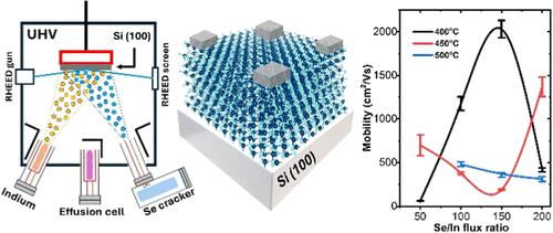
III–VI compounds, such as InxSey materials, offer an unprecedented potential for electronic devices at the atomic level. Despite their superior electronic properties, most research focused on measuring transport locally within mechanically exfoliated flakes at microscale and sometimes transferred on atomically flat surfaces. However, from a technological perspective, the integration of these materials in electronic devices requires wafer-scale, uniformly grown films, preferably integrated with the dominant semiconductor, silicon. Indium selenide films have recently shown promising electronic performance. Unfortunately, the epitaxial growth of single-phase indium selenide poses challenges due to its polymorphic nature and different stoichiometries, such as α-In2Se3, ε-for InSe, and β, γ for both InSe and In2Se3. Here, we report the growth of single phase γ-In2Se3 on Si (100), with a Hall mobility exceeding 2000 cm2/(V s) at room temperature. Our study explores the growth parameter space in the Molecular Beam Epitaxy (MBE), specifically the Se/In flux ratio and the growth temperature. It correlates them with the structural, morphological, and electrical characteristics of InxSey films. A phase map was constructed within the specified growth temperature and Se/In flux ranges. γ-In2Se3 single phase formation occurs only in a small temperature and Se/In Flux ratio window. In contrast, the formation of a mixture of γ-InSe and γ-In2Se3 phases is obtained in a large growth condition window. The sensitivity of indium selenide’s electrical and morphological properties to growth conditions implies the necessity for precise adjustments of the Se/In flux ratio alongside the growth temperature to selectively grow large-area single-phase γ-In2Se3 suitable for advanced electronic devices such as field effect transistors and photodetectors.
期刊介绍:
ACS Applied Electronic Materials is an interdisciplinary journal publishing original research covering all aspects of electronic materials. The journal is devoted to reports of new and original experimental and theoretical research of an applied nature that integrate knowledge in the areas of materials science, engineering, optics, physics, and chemistry into important applications of electronic materials. Sample research topics that span the journal's scope are inorganic, organic, ionic and polymeric materials with properties that include conducting, semiconducting, superconducting, insulating, dielectric, magnetic, optoelectronic, piezoelectric, ferroelectric and thermoelectric.
Indexed/Abstracted:
Web of Science SCIE
Scopus
CAS
INSPEC
Portico


 分享
分享
 求助内容:
求助内容: 应助结果提醒方式:
 扫码关注我们
