S. P. Zimin, I. I. Amirov, L. A. Mazaletskiy, N. N. Kolesnikov, A. V. Timonina
{"title":"不同晶向PbX (X = S, Se, Te)单晶样品的溅射产率","authors":"S. P. Zimin, I. I. Amirov, L. A. Mazaletskiy, N. N. Kolesnikov, A. V. Timonina","doi":"10.1134/S1027451024701210","DOIUrl":null,"url":null,"abstract":"<p>A study was carried out on sputtering yields for Pb<i>X</i> (<i>X</i> = S, Se, Te) single crystals with (100) orientation and PbTe and PbSe single-crystal films with (111) orientation under ion-plasma bombardment with argon ions. The Pb<i>X</i> single crystals were grown by the vertical zone melting method and oriented along the [100] growth axis. Single-crystal films of lead chalcogenides 2–4 μm thick with an orientation (111) relative to the normal to the substrate were formed by molecular beam epitaxy on silicon substrates. The surface treatment was carried out in a high-density argon plasma reactor of a high-frequency inductive discharge (13.56 MHz) of low pressure at an average ion energy of 50, 100, 150, and 200 eV. Based on the comparative analysis of sputtering rates, it was shown that for the (100) orientation, the sputtering yields for lead telluride were lower compared to lead sulfide and lead selenide. The sputtering yields for PbTe and PbSe for the (111) crystallographic orientation was found to be higher compared to (100) orientation.</p>","PeriodicalId":671,"journal":{"name":"Journal of Surface Investigation: X-ray, Synchrotron and Neutron Techniques","volume":"18 6","pages":"1326 - 1332"},"PeriodicalIF":0.4000,"publicationDate":"2025-03-01","publicationTypes":"Journal Article","fieldsOfStudy":null,"isOpenAccess":false,"openAccessPdf":"","citationCount":"0","resultStr":"{\"title\":\"Sputtering Yields for Single Crystal Samples of PbX (X = S, Se, Te) with Different Crystallographic Orientations\",\"authors\":\"S. P. Zimin, I. I. Amirov, L. A. Mazaletskiy, N. N. Kolesnikov, A. V. Timonina\",\"doi\":\"10.1134/S1027451024701210\",\"DOIUrl\":null,\"url\":null,\"abstract\":\"<p>A study was carried out on sputtering yields for Pb<i>X</i> (<i>X</i> = S, Se, Te) single crystals with (100) orientation and PbTe and PbSe single-crystal films with (111) orientation under ion-plasma bombardment with argon ions. The Pb<i>X</i> single crystals were grown by the vertical zone melting method and oriented along the [100] growth axis. Single-crystal films of lead chalcogenides 2–4 μm thick with an orientation (111) relative to the normal to the substrate were formed by molecular beam epitaxy on silicon substrates. The surface treatment was carried out in a high-density argon plasma reactor of a high-frequency inductive discharge (13.56 MHz) of low pressure at an average ion energy of 50, 100, 150, and 200 eV. Based on the comparative analysis of sputtering rates, it was shown that for the (100) orientation, the sputtering yields for lead telluride were lower compared to lead sulfide and lead selenide. The sputtering yields for PbTe and PbSe for the (111) crystallographic orientation was found to be higher compared to (100) orientation.</p>\",\"PeriodicalId\":671,\"journal\":{\"name\":\"Journal of Surface Investigation: X-ray, Synchrotron and Neutron Techniques\",\"volume\":\"18 6\",\"pages\":\"1326 - 1332\"},\"PeriodicalIF\":0.4000,\"publicationDate\":\"2025-03-01\",\"publicationTypes\":\"Journal Article\",\"fieldsOfStudy\":null,\"isOpenAccess\":false,\"openAccessPdf\":\"\",\"citationCount\":\"0\",\"resultStr\":null,\"platform\":\"Semanticscholar\",\"paperid\":null,\"PeriodicalName\":\"Journal of Surface Investigation: X-ray, Synchrotron and Neutron Techniques\",\"FirstCategoryId\":\"1085\",\"ListUrlMain\":\"https://link.springer.com/article/10.1134/S1027451024701210\",\"RegionNum\":0,\"RegionCategory\":null,\"ArticlePicture\":[],\"TitleCN\":null,\"AbstractTextCN\":null,\"PMCID\":null,\"EPubDate\":\"\",\"PubModel\":\"\",\"JCR\":\"Q4\",\"JCRName\":\"PHYSICS, CONDENSED MATTER\",\"Score\":null,\"Total\":0}","platform":"Semanticscholar","paperid":null,"PeriodicalName":"Journal of Surface Investigation: X-ray, Synchrotron and Neutron Techniques","FirstCategoryId":"1085","ListUrlMain":"https://link.springer.com/article/10.1134/S1027451024701210","RegionNum":0,"RegionCategory":null,"ArticlePicture":[],"TitleCN":null,"AbstractTextCN":null,"PMCID":null,"EPubDate":"","PubModel":"","JCR":"Q4","JCRName":"PHYSICS, CONDENSED MATTER","Score":null,"Total":0}
Sputtering Yields for Single Crystal Samples of PbX (X = S, Se, Te) with Different Crystallographic Orientations
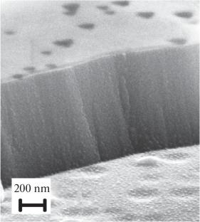
A study was carried out on sputtering yields for PbX (X = S, Se, Te) single crystals with (100) orientation and PbTe and PbSe single-crystal films with (111) orientation under ion-plasma bombardment with argon ions. The PbX single crystals were grown by the vertical zone melting method and oriented along the [100] growth axis. Single-crystal films of lead chalcogenides 2–4 μm thick with an orientation (111) relative to the normal to the substrate were formed by molecular beam epitaxy on silicon substrates. The surface treatment was carried out in a high-density argon plasma reactor of a high-frequency inductive discharge (13.56 MHz) of low pressure at an average ion energy of 50, 100, 150, and 200 eV. Based on the comparative analysis of sputtering rates, it was shown that for the (100) orientation, the sputtering yields for lead telluride were lower compared to lead sulfide and lead selenide. The sputtering yields for PbTe and PbSe for the (111) crystallographic orientation was found to be higher compared to (100) orientation.
期刊介绍:
Journal of Surface Investigation: X-ray, Synchrotron and Neutron Techniques publishes original articles on the topical problems of solid-state physics, materials science, experimental techniques, condensed media, nanostructures, surfaces of thin films, and phase boundaries: geometric and energetical structures of surfaces, the methods of computer simulations; physical and chemical properties and their changes upon radiation and other treatments; the methods of studies of films and surface layers of crystals (XRD, XPS, synchrotron radiation, neutron and electron diffraction, electron microscopic, scanning tunneling microscopic, atomic force microscopic studies, and other methods that provide data on the surfaces and thin films). Articles related to the methods and technics of structure studies are the focus of the journal. The journal accepts manuscripts of regular articles and reviews in English or Russian language from authors of all countries. All manuscripts are peer-reviewed.




 京公网安备 11010802042870号
京ICP备2023020795号-1
京公网安备 11010802042870号
京ICP备2023020795号-1

 分享
分享
 求助内容:
求助内容: 应助结果提醒方式:
 扫码关注我们
