Basit Ali , Mehrdad Karimzadehkhouei , Mohammad Nasr Esfahani , Yusuf Leblebici , B. Erdem Alaca
{"title":"用于桥接MEMS和NEMS的模板光刻","authors":"Basit Ali , Mehrdad Karimzadehkhouei , Mohammad Nasr Esfahani , Yusuf Leblebici , B. Erdem Alaca","doi":"10.1016/j.mne.2023.100206","DOIUrl":null,"url":null,"abstract":"<div><p>The damage inflicted to silicon nanowires (Si NWs) during the HF vapor etch release poses a challenge to the monolithic integration of Si NWs with higher-order structures, such as microelectromechanical systems (MEMS). This paper reports the development of a stencil lithography-based protection technology that protects Si NWs during prolonged HF vapor release and enables their MEMS integration. Besides, a simplified fabrication flow for the stencil is presented offering ease of patterning of backside features on the nitride membrane. The entire process on Si NW can be performed in a resistless manner. HF vapor etch damage to the Si NWs is characterized, followed by the calibration of the proposed technology steps for Si NW protection. The stencil is fabricated and the developed technology is applied on a Si NW-based multiscale device architecture to protectively coat Si NWs in a localized manner. Protection of Si NW under a prolonged (>3 h) HF vapor etch process has been achieved. Moreover, selective removal of the protection layer around Si NW is demonstrated at the end of the process. The proposed technology also offers access to localized surface modifications on a multiscale device architecture for biological or chemical sensing applications.</p></div>","PeriodicalId":37111,"journal":{"name":"Micro and Nano Engineering","volume":"19 ","pages":"Article 100206"},"PeriodicalIF":2.8000,"publicationDate":"2023-06-01","publicationTypes":"Journal Article","fieldsOfStudy":null,"isOpenAccess":false,"openAccessPdf":"","citationCount":"1","resultStr":"{\"title\":\"Stencil lithography for bridging MEMS and NEMS\",\"authors\":\"Basit Ali , Mehrdad Karimzadehkhouei , Mohammad Nasr Esfahani , Yusuf Leblebici , B. Erdem Alaca\",\"doi\":\"10.1016/j.mne.2023.100206\",\"DOIUrl\":null,\"url\":null,\"abstract\":\"<div><p>The damage inflicted to silicon nanowires (Si NWs) during the HF vapor etch release poses a challenge to the monolithic integration of Si NWs with higher-order structures, such as microelectromechanical systems (MEMS). This paper reports the development of a stencil lithography-based protection technology that protects Si NWs during prolonged HF vapor release and enables their MEMS integration. Besides, a simplified fabrication flow for the stencil is presented offering ease of patterning of backside features on the nitride membrane. The entire process on Si NW can be performed in a resistless manner. HF vapor etch damage to the Si NWs is characterized, followed by the calibration of the proposed technology steps for Si NW protection. The stencil is fabricated and the developed technology is applied on a Si NW-based multiscale device architecture to protectively coat Si NWs in a localized manner. Protection of Si NW under a prolonged (>3 h) HF vapor etch process has been achieved. Moreover, selective removal of the protection layer around Si NW is demonstrated at the end of the process. The proposed technology also offers access to localized surface modifications on a multiscale device architecture for biological or chemical sensing applications.</p></div>\",\"PeriodicalId\":37111,\"journal\":{\"name\":\"Micro and Nano Engineering\",\"volume\":\"19 \",\"pages\":\"Article 100206\"},\"PeriodicalIF\":2.8000,\"publicationDate\":\"2023-06-01\",\"publicationTypes\":\"Journal Article\",\"fieldsOfStudy\":null,\"isOpenAccess\":false,\"openAccessPdf\":\"\",\"citationCount\":\"1\",\"resultStr\":null,\"platform\":\"Semanticscholar\",\"paperid\":null,\"PeriodicalName\":\"Micro and Nano Engineering\",\"FirstCategoryId\":\"1085\",\"ListUrlMain\":\"https://www.sciencedirect.com/science/article/pii/S2590007223000369\",\"RegionNum\":0,\"RegionCategory\":null,\"ArticlePicture\":[],\"TitleCN\":null,\"AbstractTextCN\":null,\"PMCID\":null,\"EPubDate\":\"\",\"PubModel\":\"\",\"JCR\":\"Q2\",\"JCRName\":\"ENGINEERING, ELECTRICAL & ELECTRONIC\",\"Score\":null,\"Total\":0}","platform":"Semanticscholar","paperid":null,"PeriodicalName":"Micro and Nano Engineering","FirstCategoryId":"1085","ListUrlMain":"https://www.sciencedirect.com/science/article/pii/S2590007223000369","RegionNum":0,"RegionCategory":null,"ArticlePicture":[],"TitleCN":null,"AbstractTextCN":null,"PMCID":null,"EPubDate":"","PubModel":"","JCR":"Q2","JCRName":"ENGINEERING, ELECTRICAL & ELECTRONIC","Score":null,"Total":0}
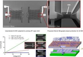
The damage inflicted to silicon nanowires (Si NWs) during the HF vapor etch release poses a challenge to the monolithic integration of Si NWs with higher-order structures, such as microelectromechanical systems (MEMS). This paper reports the development of a stencil lithography-based protection technology that protects Si NWs during prolonged HF vapor release and enables their MEMS integration. Besides, a simplified fabrication flow for the stencil is presented offering ease of patterning of backside features on the nitride membrane. The entire process on Si NW can be performed in a resistless manner. HF vapor etch damage to the Si NWs is characterized, followed by the calibration of the proposed technology steps for Si NW protection. The stencil is fabricated and the developed technology is applied on a Si NW-based multiscale device architecture to protectively coat Si NWs in a localized manner. Protection of Si NW under a prolonged (>3 h) HF vapor etch process has been achieved. Moreover, selective removal of the protection layer around Si NW is demonstrated at the end of the process. The proposed technology also offers access to localized surface modifications on a multiscale device architecture for biological or chemical sensing applications.


 分享
分享
 求助内容:
求助内容: 应助结果提醒方式:
 扫码关注我们
