S. Takase, K. Yamada, Y. Nakagawa, C. Oka, J. Sakurai, S. Hata
{"title":"使用反向剥离的厚膜MEMS工艺","authors":"S. Takase, K. Yamada, Y. Nakagawa, C. Oka, J. Sakurai, S. Hata","doi":"10.1016/j.mee.2023.112081","DOIUrl":null,"url":null,"abstract":"<div><p>The lift-off process is a microfabrication technique that has the capability of forming thin film structures. However, several issues, such as structural shape and burr formation, arise when applying this method to the formation of thick film structures. Thick film structures formed through the lift-off process exhibit a mountainous cross-sectional shape and non-uniform film thickness due to variations in the width of the structure. These challenges make it difficult to apply the method to MEMS. While the reverse lift-off process addresses some of the structural shape problems, its initial development using metal molds makes it challenging to directly apply to MEMS without modification. Therefore, this paper proposes an adaptation to the Si process and presents a method to reduce burrs. The microfabrication characteristics are evaluated by comparing the cross-sectional shapes of thick metallic glass structures formed through both the lift-off and reverse lift-off processes. The structures formed through the reverse lift-off process exhibit a rectangular cross-sectional shape, and the film thickness remains consistent regardless of the structure's width. However, burrs persist on the backside edge of the structure, which hinders its application to MEMS. This paper confirms that pre-etching the underlying Si substrate into an inverse tapered shape effectively reduces burrs. As an illustration of the improved reverse lift-off process applied to MEMS, MEMS mirror structures are fabricated, and their resonance frequency closely aligns with the design value.</p></div>","PeriodicalId":18557,"journal":{"name":"Microelectronic Engineering","volume":"281 ","pages":"Article 112081"},"PeriodicalIF":3.3000,"publicationDate":"2023-09-15","publicationTypes":"Journal Article","fieldsOfStudy":null,"isOpenAccess":false,"openAccessPdf":"","citationCount":"0","resultStr":"{\"title\":\"Thick film MEMS process using reverse lift-off\",\"authors\":\"S. Takase, K. Yamada, Y. Nakagawa, C. Oka, J. Sakurai, S. Hata\",\"doi\":\"10.1016/j.mee.2023.112081\",\"DOIUrl\":null,\"url\":null,\"abstract\":\"<div><p>The lift-off process is a microfabrication technique that has the capability of forming thin film structures. However, several issues, such as structural shape and burr formation, arise when applying this method to the formation of thick film structures. Thick film structures formed through the lift-off process exhibit a mountainous cross-sectional shape and non-uniform film thickness due to variations in the width of the structure. These challenges make it difficult to apply the method to MEMS. While the reverse lift-off process addresses some of the structural shape problems, its initial development using metal molds makes it challenging to directly apply to MEMS without modification. Therefore, this paper proposes an adaptation to the Si process and presents a method to reduce burrs. The microfabrication characteristics are evaluated by comparing the cross-sectional shapes of thick metallic glass structures formed through both the lift-off and reverse lift-off processes. The structures formed through the reverse lift-off process exhibit a rectangular cross-sectional shape, and the film thickness remains consistent regardless of the structure's width. However, burrs persist on the backside edge of the structure, which hinders its application to MEMS. This paper confirms that pre-etching the underlying Si substrate into an inverse tapered shape effectively reduces burrs. As an illustration of the improved reverse lift-off process applied to MEMS, MEMS mirror structures are fabricated, and their resonance frequency closely aligns with the design value.</p></div>\",\"PeriodicalId\":18557,\"journal\":{\"name\":\"Microelectronic Engineering\",\"volume\":\"281 \",\"pages\":\"Article 112081\"},\"PeriodicalIF\":3.3000,\"publicationDate\":\"2023-09-15\",\"publicationTypes\":\"Journal Article\",\"fieldsOfStudy\":null,\"isOpenAccess\":false,\"openAccessPdf\":\"\",\"citationCount\":\"0\",\"resultStr\":null,\"platform\":\"Semanticscholar\",\"paperid\":null,\"PeriodicalName\":\"Microelectronic Engineering\",\"FirstCategoryId\":\"5\",\"ListUrlMain\":\"https://www.sciencedirect.com/science/article/pii/S0167931723001466\",\"RegionNum\":4,\"RegionCategory\":\"工程技术\",\"ArticlePicture\":[],\"TitleCN\":null,\"AbstractTextCN\":null,\"PMCID\":null,\"EPubDate\":\"2023/8/12 0:00:00\",\"PubModel\":\"Epub\",\"JCR\":\"Q2\",\"JCRName\":\"ENGINEERING, ELECTRICAL & ELECTRONIC\",\"Score\":null,\"Total\":0}","platform":"Semanticscholar","paperid":null,"PeriodicalName":"Microelectronic Engineering","FirstCategoryId":"5","ListUrlMain":"https://www.sciencedirect.com/science/article/pii/S0167931723001466","RegionNum":4,"RegionCategory":"工程技术","ArticlePicture":[],"TitleCN":null,"AbstractTextCN":null,"PMCID":null,"EPubDate":"2023/8/12 0:00:00","PubModel":"Epub","JCR":"Q2","JCRName":"ENGINEERING, ELECTRICAL & ELECTRONIC","Score":null,"Total":0}
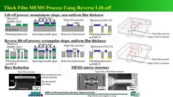
The lift-off process is a microfabrication technique that has the capability of forming thin film structures. However, several issues, such as structural shape and burr formation, arise when applying this method to the formation of thick film structures. Thick film structures formed through the lift-off process exhibit a mountainous cross-sectional shape and non-uniform film thickness due to variations in the width of the structure. These challenges make it difficult to apply the method to MEMS. While the reverse lift-off process addresses some of the structural shape problems, its initial development using metal molds makes it challenging to directly apply to MEMS without modification. Therefore, this paper proposes an adaptation to the Si process and presents a method to reduce burrs. The microfabrication characteristics are evaluated by comparing the cross-sectional shapes of thick metallic glass structures formed through both the lift-off and reverse lift-off processes. The structures formed through the reverse lift-off process exhibit a rectangular cross-sectional shape, and the film thickness remains consistent regardless of the structure's width. However, burrs persist on the backside edge of the structure, which hinders its application to MEMS. This paper confirms that pre-etching the underlying Si substrate into an inverse tapered shape effectively reduces burrs. As an illustration of the improved reverse lift-off process applied to MEMS, MEMS mirror structures are fabricated, and their resonance frequency closely aligns with the design value.
期刊介绍:
Microelectronic Engineering is the premier nanoprocessing, and nanotechnology journal focusing on fabrication of electronic, photonic, bioelectronic, electromechanic and fluidic devices and systems, and their applications in the broad areas of electronics, photonics, energy, life sciences, and environment. It covers also the expanding interdisciplinary field of "more than Moore" and "beyond Moore" integrated nanoelectronics / photonics and micro-/nano-/bio-systems. Through its unique mixture of peer-reviewed articles, reviews, accelerated publications, short and Technical notes, and the latest research news on key developments, Microelectronic Engineering provides comprehensive coverage of this exciting, interdisciplinary and dynamic new field for researchers in academia and professionals in industry.


 分享
分享
 求助内容:
求助内容: 应助结果提醒方式:
 扫码关注我们
