Rijo Baby , Manish Mandal , Shamibrota K. Roy , Abheek Bardhan , Rangarajan Muralidharan , Kaushik Basu , Srinivasan Raghavan , Digbijoy N. Nath
{"title":"8. A、 200 硅HEMT上V常关共源共栅GaN:从外延到双脉冲测试","authors":"Rijo Baby , Manish Mandal , Shamibrota K. Roy , Abheek Bardhan , Rangarajan Muralidharan , Kaushik Basu , Srinivasan Raghavan , Digbijoy N. Nath","doi":"10.1016/j.mee.2023.112085","DOIUrl":null,"url":null,"abstract":"<div><p><span><span>In this paper, we provide a comprehensive study on all aspects of development of normally-off multi-finger III-nitride HEMT on </span>Silicon<span> in cascode configuration. AlGaN/GaN HEMT epi-stack with in situ SiN cap was grown on 2-in. Silicon (111) using MOCVD<span><span><span>, utilizing a 2-step AlN nucleation, step-graded AlGaN transition layer and C-doped GaN buffer. Depletion-mode HEMTs in winding gate geometry with a gate width of 30 mm were fabricated with thick electroplated metal contacts and an optimized bilayer SiN </span>passivation<span>. Devices were diced and packaged in TO254 with conducting epoxy and Au-coated ceramic substrate. These packaged D-mode HEMTs exhibited a </span></span>threshold voltage (V</span></span></span><sub>th</sub><span>) of −12 V, maximum ON current of 10 A, and a 3-terminal hard breakdown in excess of 400 V. Bare dies of D-mode HEMTs were then integrated with commercially procured silicon MOSFET in a TO254 package in cascode configuration to achieve V</span><sub>th</sub> > 2 V, ON current of 8 A, and breakdown >200 V. The normally-off cascaded GaN HEMTs were subjected to various gate and drain stress measurements and were found to exhibit a V<sub>th</sub><span><span> shift of 10 mV after 1000 s of positive gate (+5 V) stress. The input and output capacitances of the cascode devices were measured to be 1 nF and 0.8 nF, respectively. The 3rd quadrant operation was checked at 8 A on-state current level to reveal a lower voltage drop of 0.7 V. Finally, cascode HEMTs were subjected to double pulsed testing (DPT) using a half-bridge evaluation board. On and off rise times of 52 ns and 59 ns were obtained along with </span>energy loss of 25 μJ and 20 μJ, respectively, for devices switched at 8 A, 100 V.</span></p></div>","PeriodicalId":18557,"journal":{"name":"Microelectronic Engineering","volume":"282 ","pages":"Article 112085"},"PeriodicalIF":3.1000,"publicationDate":"2023-10-15","publicationTypes":"Journal Article","fieldsOfStudy":null,"isOpenAccess":false,"openAccessPdf":"","citationCount":"0","resultStr":"{\"title\":\"8 A, 200 V normally-off cascode GaN-on-Si HEMT: From epitaxy to double pulse testing\",\"authors\":\"Rijo Baby , Manish Mandal , Shamibrota K. Roy , Abheek Bardhan , Rangarajan Muralidharan , Kaushik Basu , Srinivasan Raghavan , Digbijoy N. Nath\",\"doi\":\"10.1016/j.mee.2023.112085\",\"DOIUrl\":null,\"url\":null,\"abstract\":\"<div><p><span><span>In this paper, we provide a comprehensive study on all aspects of development of normally-off multi-finger III-nitride HEMT on </span>Silicon<span> in cascode configuration. AlGaN/GaN HEMT epi-stack with in situ SiN cap was grown on 2-in. Silicon (111) using MOCVD<span><span><span>, utilizing a 2-step AlN nucleation, step-graded AlGaN transition layer and C-doped GaN buffer. Depletion-mode HEMTs in winding gate geometry with a gate width of 30 mm were fabricated with thick electroplated metal contacts and an optimized bilayer SiN </span>passivation<span>. Devices were diced and packaged in TO254 with conducting epoxy and Au-coated ceramic substrate. These packaged D-mode HEMTs exhibited a </span></span>threshold voltage (V</span></span></span><sub>th</sub><span>) of −12 V, maximum ON current of 10 A, and a 3-terminal hard breakdown in excess of 400 V. Bare dies of D-mode HEMTs were then integrated with commercially procured silicon MOSFET in a TO254 package in cascode configuration to achieve V</span><sub>th</sub> > 2 V, ON current of 8 A, and breakdown >200 V. The normally-off cascaded GaN HEMTs were subjected to various gate and drain stress measurements and were found to exhibit a V<sub>th</sub><span><span> shift of 10 mV after 1000 s of positive gate (+5 V) stress. The input and output capacitances of the cascode devices were measured to be 1 nF and 0.8 nF, respectively. The 3rd quadrant operation was checked at 8 A on-state current level to reveal a lower voltage drop of 0.7 V. Finally, cascode HEMTs were subjected to double pulsed testing (DPT) using a half-bridge evaluation board. On and off rise times of 52 ns and 59 ns were obtained along with </span>energy loss of 25 μJ and 20 μJ, respectively, for devices switched at 8 A, 100 V.</span></p></div>\",\"PeriodicalId\":18557,\"journal\":{\"name\":\"Microelectronic Engineering\",\"volume\":\"282 \",\"pages\":\"Article 112085\"},\"PeriodicalIF\":3.1000,\"publicationDate\":\"2023-10-15\",\"publicationTypes\":\"Journal Article\",\"fieldsOfStudy\":null,\"isOpenAccess\":false,\"openAccessPdf\":\"\",\"citationCount\":\"0\",\"resultStr\":null,\"platform\":\"Semanticscholar\",\"paperid\":null,\"PeriodicalName\":\"Microelectronic Engineering\",\"FirstCategoryId\":\"5\",\"ListUrlMain\":\"https://www.sciencedirect.com/science/article/pii/S0167931723001508\",\"RegionNum\":4,\"RegionCategory\":\"工程技术\",\"ArticlePicture\":[],\"TitleCN\":null,\"AbstractTextCN\":null,\"PMCID\":null,\"EPubDate\":\"2023/8/19 0:00:00\",\"PubModel\":\"Epub\",\"JCR\":\"Q2\",\"JCRName\":\"ENGINEERING, ELECTRICAL & ELECTRONIC\",\"Score\":null,\"Total\":0}","platform":"Semanticscholar","paperid":null,"PeriodicalName":"Microelectronic Engineering","FirstCategoryId":"5","ListUrlMain":"https://www.sciencedirect.com/science/article/pii/S0167931723001508","RegionNum":4,"RegionCategory":"工程技术","ArticlePicture":[],"TitleCN":null,"AbstractTextCN":null,"PMCID":null,"EPubDate":"2023/8/19 0:00:00","PubModel":"Epub","JCR":"Q2","JCRName":"ENGINEERING, ELECTRICAL & ELECTRONIC","Score":null,"Total":0}
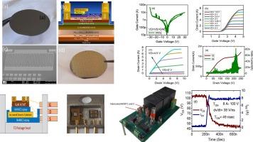
8 A, 200 V normally-off cascode GaN-on-Si HEMT: From epitaxy to double pulse testing
In this paper, we provide a comprehensive study on all aspects of development of normally-off multi-finger III-nitride HEMT on Silicon in cascode configuration. AlGaN/GaN HEMT epi-stack with in situ SiN cap was grown on 2-in. Silicon (111) using MOCVD, utilizing a 2-step AlN nucleation, step-graded AlGaN transition layer and C-doped GaN buffer. Depletion-mode HEMTs in winding gate geometry with a gate width of 30 mm were fabricated with thick electroplated metal contacts and an optimized bilayer SiN passivation. Devices were diced and packaged in TO254 with conducting epoxy and Au-coated ceramic substrate. These packaged D-mode HEMTs exhibited a threshold voltage (Vth) of −12 V, maximum ON current of 10 A, and a 3-terminal hard breakdown in excess of 400 V. Bare dies of D-mode HEMTs were then integrated with commercially procured silicon MOSFET in a TO254 package in cascode configuration to achieve Vth > 2 V, ON current of 8 A, and breakdown >200 V. The normally-off cascaded GaN HEMTs were subjected to various gate and drain stress measurements and were found to exhibit a Vth shift of 10 mV after 1000 s of positive gate (+5 V) stress. The input and output capacitances of the cascode devices were measured to be 1 nF and 0.8 nF, respectively. The 3rd quadrant operation was checked at 8 A on-state current level to reveal a lower voltage drop of 0.7 V. Finally, cascode HEMTs were subjected to double pulsed testing (DPT) using a half-bridge evaluation board. On and off rise times of 52 ns and 59 ns were obtained along with energy loss of 25 μJ and 20 μJ, respectively, for devices switched at 8 A, 100 V.
期刊介绍:
Microelectronic Engineering is the premier nanoprocessing, and nanotechnology journal focusing on fabrication of electronic, photonic, bioelectronic, electromechanic and fluidic devices and systems, and their applications in the broad areas of electronics, photonics, energy, life sciences, and environment. It covers also the expanding interdisciplinary field of "more than Moore" and "beyond Moore" integrated nanoelectronics / photonics and micro-/nano-/bio-systems. Through its unique mixture of peer-reviewed articles, reviews, accelerated publications, short and Technical notes, and the latest research news on key developments, Microelectronic Engineering provides comprehensive coverage of this exciting, interdisciplinary and dynamic new field for researchers in academia and professionals in industry.


 分享
分享
 求助内容:
求助内容: 应助结果提醒方式:
 扫码关注我们
