Anatoly Druzhinin, Igor Kogut, Victor Holota, Stepan Nichkalo, Yuriy Khoverko, Taras Benko
{"title":"降低 CMOS 逆变器开关能量的方法","authors":"Anatoly Druzhinin, Igor Kogut, Victor Holota, Stepan Nichkalo, Yuriy Khoverko, Taras Benko","doi":"10.1007/s13204-023-02929-9","DOIUrl":null,"url":null,"abstract":"<div><p>In CMOS inverters, the main part of the power supply is spent on charging the parasitic capacitance of the transistor gates and the load capacitance. Associated with this portion of energy is dynamic power consumption, which has two components—transient power consumption and capacitive-load power consumption. When the logic states of the inverter change in a short period of time, when the PMOS and NMOS transistors are switched simultaneously, a short-circuit current flows. Power losses from short-circuit current are only a small part of dynamic power consumption. For this reason, more attention is paid to reducing transient power consumption and capacitive-load power consumption. However, with the reduction in the size of the inverter transistors and the lowering of their threshold voltage, the short-circuit power losses must also be taken into account. Also, when the size of inverter transistors increases in powerful output buffers, the short-circuit current increases, which, in addition to increasing short-circuit power losses, can cause errors in the output logic. Therefore, the purpose of this work is to reduce short-circuit current and dynamic power consumption of the CMOS inverter. For this purpose, it is proposed to limit the short-circuit current by changing the state of additional PMOS and NMOS transistors included in the path of the short-circuit current. The state of additional transistors is changed by an additional clock signal with a special wave-form during the rising and falling edges of the main clock signal.</p></div>","PeriodicalId":471,"journal":{"name":"Applied Nanoscience","volume":"13 12","pages":"7501 - 7511"},"PeriodicalIF":3.6740,"publicationDate":"2023-08-11","publicationTypes":"Journal Article","fieldsOfStudy":null,"isOpenAccess":false,"openAccessPdf":"","citationCount":"0","resultStr":"{\"title\":\"The method of reducing the CMOS inverter switching energy\",\"authors\":\"Anatoly Druzhinin, Igor Kogut, Victor Holota, Stepan Nichkalo, Yuriy Khoverko, Taras Benko\",\"doi\":\"10.1007/s13204-023-02929-9\",\"DOIUrl\":null,\"url\":null,\"abstract\":\"<div><p>In CMOS inverters, the main part of the power supply is spent on charging the parasitic capacitance of the transistor gates and the load capacitance. Associated with this portion of energy is dynamic power consumption, which has two components—transient power consumption and capacitive-load power consumption. When the logic states of the inverter change in a short period of time, when the PMOS and NMOS transistors are switched simultaneously, a short-circuit current flows. Power losses from short-circuit current are only a small part of dynamic power consumption. For this reason, more attention is paid to reducing transient power consumption and capacitive-load power consumption. However, with the reduction in the size of the inverter transistors and the lowering of their threshold voltage, the short-circuit power losses must also be taken into account. Also, when the size of inverter transistors increases in powerful output buffers, the short-circuit current increases, which, in addition to increasing short-circuit power losses, can cause errors in the output logic. Therefore, the purpose of this work is to reduce short-circuit current and dynamic power consumption of the CMOS inverter. For this purpose, it is proposed to limit the short-circuit current by changing the state of additional PMOS and NMOS transistors included in the path of the short-circuit current. The state of additional transistors is changed by an additional clock signal with a special wave-form during the rising and falling edges of the main clock signal.</p></div>\",\"PeriodicalId\":471,\"journal\":{\"name\":\"Applied Nanoscience\",\"volume\":\"13 12\",\"pages\":\"7501 - 7511\"},\"PeriodicalIF\":3.6740,\"publicationDate\":\"2023-08-11\",\"publicationTypes\":\"Journal Article\",\"fieldsOfStudy\":null,\"isOpenAccess\":false,\"openAccessPdf\":\"\",\"citationCount\":\"0\",\"resultStr\":null,\"platform\":\"Semanticscholar\",\"paperid\":null,\"PeriodicalName\":\"Applied Nanoscience\",\"FirstCategoryId\":\"5\",\"ListUrlMain\":\"https://link.springer.com/article/10.1007/s13204-023-02929-9\",\"RegionNum\":4,\"RegionCategory\":\"工程技术\",\"ArticlePicture\":[],\"TitleCN\":null,\"AbstractTextCN\":null,\"PMCID\":null,\"EPubDate\":\"\",\"PubModel\":\"\",\"JCR\":\"Q1\",\"JCRName\":\"Engineering\",\"Score\":null,\"Total\":0}","platform":"Semanticscholar","paperid":null,"PeriodicalName":"Applied Nanoscience","FirstCategoryId":"5","ListUrlMain":"https://link.springer.com/article/10.1007/s13204-023-02929-9","RegionNum":4,"RegionCategory":"工程技术","ArticlePicture":[],"TitleCN":null,"AbstractTextCN":null,"PMCID":null,"EPubDate":"","PubModel":"","JCR":"Q1","JCRName":"Engineering","Score":null,"Total":0}
The method of reducing the CMOS inverter switching energy
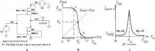
In CMOS inverters, the main part of the power supply is spent on charging the parasitic capacitance of the transistor gates and the load capacitance. Associated with this portion of energy is dynamic power consumption, which has two components—transient power consumption and capacitive-load power consumption. When the logic states of the inverter change in a short period of time, when the PMOS and NMOS transistors are switched simultaneously, a short-circuit current flows. Power losses from short-circuit current are only a small part of dynamic power consumption. For this reason, more attention is paid to reducing transient power consumption and capacitive-load power consumption. However, with the reduction in the size of the inverter transistors and the lowering of their threshold voltage, the short-circuit power losses must also be taken into account. Also, when the size of inverter transistors increases in powerful output buffers, the short-circuit current increases, which, in addition to increasing short-circuit power losses, can cause errors in the output logic. Therefore, the purpose of this work is to reduce short-circuit current and dynamic power consumption of the CMOS inverter. For this purpose, it is proposed to limit the short-circuit current by changing the state of additional PMOS and NMOS transistors included in the path of the short-circuit current. The state of additional transistors is changed by an additional clock signal with a special wave-form during the rising and falling edges of the main clock signal.
期刊介绍:
Applied Nanoscience is a hybrid journal that publishes original articles about state of the art nanoscience and the application of emerging nanotechnologies to areas fundamental to building technologically advanced and sustainable civilization, including areas as diverse as water science, advanced materials, energy, electronics, environmental science and medicine. The journal accepts original and review articles as well as book reviews for publication. All the manuscripts are single-blind peer-reviewed for scientific quality and acceptance.


 分享
分享
 求助内容:
求助内容: 应助结果提醒方式:
 扫码关注我们
