{"title":"基于势垒带工程方法的高性能中波红外inassb nBn光电探测器的设计与建模。","authors":"Maryam Shaveisi, Peiman Aliparast","doi":"10.1007/s12200-023-00060-9","DOIUrl":null,"url":null,"abstract":"<p><p>We report a new nBn photodetector (nBn-PD) design based on the InAlSb/AlSb/InAlSb/InAsSb material systems for mid-wavelength infrared (MWIR) applications. In this structure, delta-doped compositionally graded barrier (δ-DCGB) layers are suggested, the advantage of which is creation of a near zero valence band offset in nBn photodetectors. The design of the δ-DCGB nBn-PD device includes a 3 µm absorber layer (n-InAs<sub>0.81</sub>Sb<sub>0.19</sub>), a unipolar barrier layer (AlSb), and 0.2 μm contact layer (n-InAs<sub>0.81</sub>Sb<sub>0.19</sub>) as well as a 0.116 µm linear grading region (InAlSb) from the contact to the barrier layer and also from the barrier to the absorber layer. The analysis includes various dark current contributions, such as the Shockley-Read-Hall (SRH), trap-assisted tunneling (TAT), Auger, and Radiative recombination mechanisms, to acquire more precise results. Consequently, we show that the method used in the nBn device design leads to diffusion-limited dark current so that the dark current density is 2.596 × 10<sup>-8</sup> A/cm<sup>2</sup> at 150 K and a bias voltage of - 0.2 V. The proposed nBn detector exhibits a 50% cutoff wavelength of more than 5 µm, the peak current responsivity is 1.6 A/W at a wavelength of 4.5 µm and a - 0.2 V bias with 0.05 W/cm<sup>2</sup> backside illumination without anti-reflective coating. The maximum quantum efficiency at 4.5 µm is about 48.6%, and peak specific detectivity (D*) is of 3.37 × 10<sup>10</sup> cm⋅Hz<sup>1/2</sup>/W. Next, to solve the reflection concern in this nBn devices, we use a BaF<sub>2</sub> anti-reflection coating layer due to its high transmittance in the MWIR window. It leads to an increase of almost 100% in the optical response metrics, such as the current responsivity, quantum efficiency, and detectivity, compared to the optical response without an anti-reflection coating layer.</p>","PeriodicalId":12685,"journal":{"name":"Frontiers of Optoelectronics","volume":"16 1","pages":"5"},"PeriodicalIF":5.2000,"publicationDate":"2023-04-06","publicationTypes":"Journal Article","fieldsOfStudy":null,"isOpenAccess":false,"openAccessPdf":"https://www.ncbi.nlm.nih.gov/pmc/articles/PMC10079799/pdf/","citationCount":"1","resultStr":"{\"title\":\"Design and modeling of high-performance mid-wave infrared InAsSb-based nBn photodetector using barrier band engineering approaches.\",\"authors\":\"Maryam Shaveisi, Peiman Aliparast\",\"doi\":\"10.1007/s12200-023-00060-9\",\"DOIUrl\":null,\"url\":null,\"abstract\":\"<p><p>We report a new nBn photodetector (nBn-PD) design based on the InAlSb/AlSb/InAlSb/InAsSb material systems for mid-wavelength infrared (MWIR) applications. In this structure, delta-doped compositionally graded barrier (δ-DCGB) layers are suggested, the advantage of which is creation of a near zero valence band offset in nBn photodetectors. The design of the δ-DCGB nBn-PD device includes a 3 µm absorber layer (n-InAs<sub>0.81</sub>Sb<sub>0.19</sub>), a unipolar barrier layer (AlSb), and 0.2 μm contact layer (n-InAs<sub>0.81</sub>Sb<sub>0.19</sub>) as well as a 0.116 µm linear grading region (InAlSb) from the contact to the barrier layer and also from the barrier to the absorber layer. The analysis includes various dark current contributions, such as the Shockley-Read-Hall (SRH), trap-assisted tunneling (TAT), Auger, and Radiative recombination mechanisms, to acquire more precise results. Consequently, we show that the method used in the nBn device design leads to diffusion-limited dark current so that the dark current density is 2.596 × 10<sup>-8</sup> A/cm<sup>2</sup> at 150 K and a bias voltage of - 0.2 V. The proposed nBn detector exhibits a 50% cutoff wavelength of more than 5 µm, the peak current responsivity is 1.6 A/W at a wavelength of 4.5 µm and a - 0.2 V bias with 0.05 W/cm<sup>2</sup> backside illumination without anti-reflective coating. The maximum quantum efficiency at 4.5 µm is about 48.6%, and peak specific detectivity (D*) is of 3.37 × 10<sup>10</sup> cm⋅Hz<sup>1/2</sup>/W. Next, to solve the reflection concern in this nBn devices, we use a BaF<sub>2</sub> anti-reflection coating layer due to its high transmittance in the MWIR window. It leads to an increase of almost 100% in the optical response metrics, such as the current responsivity, quantum efficiency, and detectivity, compared to the optical response without an anti-reflection coating layer.</p>\",\"PeriodicalId\":12685,\"journal\":{\"name\":\"Frontiers of Optoelectronics\",\"volume\":\"16 1\",\"pages\":\"5\"},\"PeriodicalIF\":5.2000,\"publicationDate\":\"2023-04-06\",\"publicationTypes\":\"Journal Article\",\"fieldsOfStudy\":null,\"isOpenAccess\":false,\"openAccessPdf\":\"https://www.ncbi.nlm.nih.gov/pmc/articles/PMC10079799/pdf/\",\"citationCount\":\"1\",\"resultStr\":null,\"platform\":\"Semanticscholar\",\"paperid\":null,\"PeriodicalName\":\"Frontiers of Optoelectronics\",\"FirstCategoryId\":\"5\",\"ListUrlMain\":\"https://doi.org/10.1007/s12200-023-00060-9\",\"RegionNum\":3,\"RegionCategory\":\"工程技术\",\"ArticlePicture\":[],\"TitleCN\":null,\"AbstractTextCN\":null,\"PMCID\":null,\"EPubDate\":\"\",\"PubModel\":\"\",\"JCR\":\"Q2\",\"JCRName\":\"ENGINEERING, ELECTRICAL & ELECTRONIC\",\"Score\":null,\"Total\":0}","platform":"Semanticscholar","paperid":null,"PeriodicalName":"Frontiers of Optoelectronics","FirstCategoryId":"5","ListUrlMain":"https://doi.org/10.1007/s12200-023-00060-9","RegionNum":3,"RegionCategory":"工程技术","ArticlePicture":[],"TitleCN":null,"AbstractTextCN":null,"PMCID":null,"EPubDate":"","PubModel":"","JCR":"Q2","JCRName":"ENGINEERING, ELECTRICAL & ELECTRONIC","Score":null,"Total":0}
Design and modeling of high-performance mid-wave infrared InAsSb-based nBn photodetector using barrier band engineering approaches.
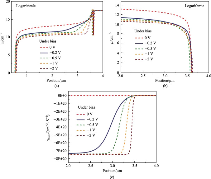
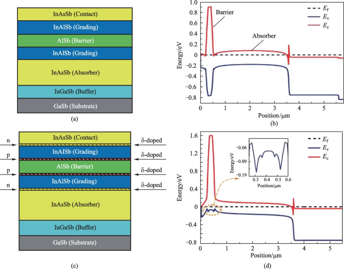
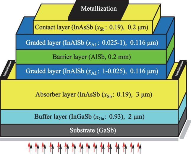
We report a new nBn photodetector (nBn-PD) design based on the InAlSb/AlSb/InAlSb/InAsSb material systems for mid-wavelength infrared (MWIR) applications. In this structure, delta-doped compositionally graded barrier (δ-DCGB) layers are suggested, the advantage of which is creation of a near zero valence band offset in nBn photodetectors. The design of the δ-DCGB nBn-PD device includes a 3 µm absorber layer (n-InAs0.81Sb0.19), a unipolar barrier layer (AlSb), and 0.2 μm contact layer (n-InAs0.81Sb0.19) as well as a 0.116 µm linear grading region (InAlSb) from the contact to the barrier layer and also from the barrier to the absorber layer. The analysis includes various dark current contributions, such as the Shockley-Read-Hall (SRH), trap-assisted tunneling (TAT), Auger, and Radiative recombination mechanisms, to acquire more precise results. Consequently, we show that the method used in the nBn device design leads to diffusion-limited dark current so that the dark current density is 2.596 × 10⁻⁸ A/cm2 at 150 K and a bias voltage of - 0.2 V. The proposed nBn detector exhibits a 50% cutoff wavelength of more than 5 µm, the peak current responsivity is 1.6 A/W at a wavelength of 4.5 µm and a - 0.2 V bias with 0.05 W/cm2 backside illumination without anti-reflective coating. The maximum quantum efficiency at 4.5 µm is about 48.6%, and peak specific detectivity (D*) is of 3.37 × 1010 cm⋅Hz1/2/W. Next, to solve the reflection concern in this nBn devices, we use a BaF2 anti-reflection coating layer due to its high transmittance in the MWIR window. It leads to an increase of almost 100% in the optical response metrics, such as the current responsivity, quantum efficiency, and detectivity, compared to the optical response without an anti-reflection coating layer.
期刊介绍:
Frontiers of Optoelectronics seeks to provide a multidisciplinary forum for a broad mix of peer-reviewed academic papers in order to promote rapid communication and exchange between researchers in China and abroad. It introduces and reflects significant achievements being made in the field of photonics or optoelectronics. The topics include, but are not limited to, semiconductor optoelectronics, nano-photonics, information photonics, energy photonics, ultrafast photonics, biomedical photonics, nonlinear photonics, fiber optics, laser and terahertz technology and intelligent photonics. The journal publishes reviews, research articles, letters, comments, special issues and so on.
Frontiers of Optoelectronics especially encourages papers from new emerging and multidisciplinary areas, papers reflecting the international trends of research and development, and on special topics reporting progress made in the field of optoelectronics. All published papers will reflect the original thoughts of researchers and practitioners on basic theories, design and new technology in optoelectronics.
Frontiers of Optoelectronics is strictly peer-reviewed and only accepts original submissions in English. It is a fully OA journal and the APCs are covered by Higher Education Press and Huazhong University of Science and Technology.
● Presents the latest developments in optoelectronics and optics
● Emphasizes the latest developments of new optoelectronic materials, devices, systems and applications
● Covers industrial photonics, information photonics, biomedical photonics, energy photonics, laser and terahertz technology, and more


 分享
分享
 求助内容:
求助内容: 应助结果提醒方式:
 扫码关注我们
