{"title":"Ta/Al/CuW low temperature ohmic contacts for GaN-on-Si HEMT","authors":"Zijing Xie , Nianhe Xiong , Jun Tang , Hong Wang","doi":"10.1016/j.mee.2024.112132","DOIUrl":null,"url":null,"abstract":"<div><p><span>We proposed a low temperature Au-free ohmic contacts<span><span> of GaN-on-Si HEMT with the Ta/Al/CuW metal stack. The CuW was deposited by using the dual-target </span>magnetron<span><span> sputter deposition method<span>. The annealing conditions and recess depth of ohmic area were systematically investigated. By utilizing the Ta/Al/CuW structure, an improved contact characteristic (0.49 Ω·mm) is obtained following annealing at 550 °C for 10 min in vacuum, with the recess depth of 30 nm(±2 nm). This performance surpasses that of Ta/Al/W Au-free contacts (1.07 Ω·mm). Furthermore, both the Ta/Al/CuW ohmic contacts (RMS = 6.3 nm) and the Ta/Al/W ohmic contacts (RMS = 6.0 nm) exhibit smooth surface morphology. Compared to Ti contact layer, Ta demonstrates superior performance in low temperature contact and breakdown test. </span></span>Amorphous Ta layer can effectively suppress Cu </span></span></span>diffusion. The GaN-on-Si HEMT was also fabricated based on Ta/Al/CuW Au-free ohmic contacts, exhibiting excellent DC characteristics.</p></div>","PeriodicalId":18557,"journal":{"name":"Microelectronic Engineering","volume":"286 ","pages":"Article 112132"},"PeriodicalIF":3.1000,"publicationDate":"2024-03-01","publicationTypes":"Journal Article","fieldsOfStudy":null,"isOpenAccess":false,"openAccessPdf":"","citationCount":"0","resultStr":null,"platform":"Semanticscholar","paperid":null,"PeriodicalName":"Microelectronic Engineering","FirstCategoryId":"5","ListUrlMain":"https://www.sciencedirect.com/science/article/pii/S0167931724000017","RegionNum":4,"RegionCategory":"工程技术","ArticlePicture":[],"TitleCN":null,"AbstractTextCN":null,"PMCID":null,"EPubDate":"2024/1/3 0:00:00","PubModel":"Epub","JCR":"Q2","JCRName":"ENGINEERING, ELECTRICAL & ELECTRONIC","Score":null,"Total":0}
引用次数: 0
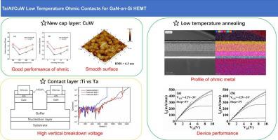
Abstract
We proposed a low temperature Au-free ohmic contacts of GaN-on-Si HEMT with the Ta/Al/CuW metal stack. The CuW was deposited by using the dual-target magnetron sputter deposition method. The annealing conditions and recess depth of ohmic area were systematically investigated. By utilizing the Ta/Al/CuW structure, an improved contact characteristic (0.49 Ω·mm) is obtained following annealing at 550 °C for 10 min in vacuum, with the recess depth of 30 nm(±2 nm). This performance surpasses that of Ta/Al/W Au-free contacts (1.07 Ω·mm). Furthermore, both the Ta/Al/CuW ohmic contacts (RMS = 6.3 nm) and the Ta/Al/W ohmic contacts (RMS = 6.0 nm) exhibit smooth surface morphology. Compared to Ti contact layer, Ta demonstrates superior performance in low temperature contact and breakdown test. Amorphous Ta layer can effectively suppress Cu diffusion. The GaN-on-Si HEMT was also fabricated based on Ta/Al/CuW Au-free ohmic contacts, exhibiting excellent DC characteristics.
期刊介绍:
Microelectronic Engineering is the premier nanoprocessing, and nanotechnology journal focusing on fabrication of electronic, photonic, bioelectronic, electromechanic and fluidic devices and systems, and their applications in the broad areas of electronics, photonics, energy, life sciences, and environment. It covers also the expanding interdisciplinary field of "more than Moore" and "beyond Moore" integrated nanoelectronics / photonics and micro-/nano-/bio-systems. Through its unique mixture of peer-reviewed articles, reviews, accelerated publications, short and Technical notes, and the latest research news on key developments, Microelectronic Engineering provides comprehensive coverage of this exciting, interdisciplinary and dynamic new field for researchers in academia and professionals in industry.


 分享
分享
 求助内容:
求助内容: 应助结果提醒方式:
 扫码关注我们
