Triple-metal gate work function engineering to improve the performance of junctionless cylindrical gate-all-around Si nanowire MOSFETs for the upcoming sub-3-nm technology node
{"title":"Triple-metal gate work function engineering to improve the performance of junctionless cylindrical gate-all-around Si nanowire MOSFETs for the upcoming sub-3-nm technology node","authors":"Sanjay, Vibhor Kumar, Anil Vohra","doi":"10.1007/s10825-024-02148-7","DOIUrl":null,"url":null,"abstract":"<div><p>Moore’s law, along with the International Roadmap for Devices and Systems, continues to guide the scaling of devices below 10 nm. The challenges posed by such small-dimensioned devices form the basis of the present work. A junctionless MOSFET with a triple-metal gate structure is proposed as an alternative to conventional single-gate bulk MOSFETs for future CMOS technology. The present work investigated the direct current and analog/radio frequency characteristics including the drain current <span>\\(({I}_{{\\text{D}}}\\)</span>), transconductance <span>\\({(g}_{m})\\)</span>, transconductance generation factor (TGF), cut-off frequency <span>\\({(f}_{T})\\)</span>, frequency–transconductance product (FTP), transit time <span>\\((\\tau ),\\)</span> and the total resistance of the source region, drain region, and channel <span>\\({(R}_{{\\text{SD}}+{\\text{CH}}})\\)</span> for triple-metal (TM) inversion-mode (IM) and junctionless (JL) cylindrical gate-all-around (CGAA) silicon nanowire (SiNW) MOSFETs with 3-nm gate length using the Silvaco ATLAS 3D TCAD tool. The non-equilibrium Green’s function and the self-consistent solution of the Schrödinger and Poisson equations were considered. The channel was taken to be lightly doped in the case of the IM TM CGAA SiNW device. The effect of the TM gate work function engineering for a SiNW channel with a diameter of 3 nm and gate oxide <span>\\(({{{\\text{Al}}}_{2}{\\text{O}}}_{3})\\)</span> thickness of 0.8 nm was investigated with respect to <span>\\({I}_{D}\\)</span>,<span>\\({ g}_{m}\\)</span>, TGF, <span>\\({f}_{T}\\)</span>, <span>\\(\\tau\\)</span>, FTP, and <span>\\({R}_{{\\text{SD}}+{\\text{CH}}}\\)</span>, and a comparative study between the IM TM and JL TM CGAA SiNW devices was carried out with respect to these parameters. For the JL device, optimization of the doping concentration was performed to obtain the same (i) <i>I</i><sub>ON</sub> current and (ii) threshold voltage (<i>V</i><sub>TH</sub>) as the IM device. An 8.61- and 5.72-fold reduction in <i>I</i><sub>OFF</sub> was seen for the same <i>I</i><sub>ON</sub> and <i>V</i><sub>TH</sub> for the JL versus the IM device. It was found that the TM gate variation led to a reduction in drain-induced barrier lowering (DIBL) in the IM and JL devices. The JL SiNW showed much lower DIBL of ~39.49 mV/V, a near-ideal subthreshold slope (SS) of ~60 mV/dec, and higher <span>\\({{\\text{I}}}_{{\\text{ON}}}/{{\\text{I}}}_{{\\text{OFF}}}\\)</span> current ratio of ~2.98 × 10<sup>12</sup>. which is much better than the values reported in the literature for CGAA devices. Also, the JL SiNW device was found to perform better than the IM SiNW device in terms of SS, DIBL, <span>\\({{\\text{I}}}_{{\\text{ON}}}/{{\\text{I}}}_{{\\text{OFF}}}\\)</span>, <span>\\({g}_{m},\\)</span> TGF, <i>f</i><sub><i>T</i></sub>, <span>\\(\\tau\\)</span>, FTP, and <span>\\({R}_{{\\text{SD}}+{\\text{CH}}}\\)</span>.</p></div>","PeriodicalId":620,"journal":{"name":"Journal of Computational Electronics","volume":"23 2","pages":"267 - 278"},"PeriodicalIF":2.5000,"publicationDate":"2024-04-15","publicationTypes":"Journal Article","fieldsOfStudy":null,"isOpenAccess":false,"openAccessPdf":"","citationCount":"0","resultStr":null,"platform":"Semanticscholar","paperid":null,"PeriodicalName":"Journal of Computational Electronics","FirstCategoryId":"5","ListUrlMain":"https://link.springer.com/article/10.1007/s10825-024-02148-7","RegionNum":4,"RegionCategory":"工程技术","ArticlePicture":[],"TitleCN":null,"AbstractTextCN":null,"PMCID":null,"EPubDate":"","PubModel":"","JCR":"Q3","JCRName":"ENGINEERING, ELECTRICAL & ELECTRONIC","Score":null,"Total":0}
引用次数: 0
Abstract
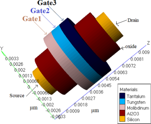
Moore’s law, along with the International Roadmap for Devices and Systems, continues to guide the scaling of devices below 10 nm. The challenges posed by such small-dimensioned devices form the basis of the present work. A junctionless MOSFET with a triple-metal gate structure is proposed as an alternative to conventional single-gate bulk MOSFETs for future CMOS technology. The present work investigated the direct current and analog/radio frequency characteristics including the drain current \(({I}_{{\text{D}}}\)), transconductance \({(g}_{m})\), transconductance generation factor (TGF), cut-off frequency \({(f}_{T})\), frequency–transconductance product (FTP), transit time \((\tau ),\) and the total resistance of the source region, drain region, and channel \({(R}_{{\text{SD}}+{\text{CH}}})\) for triple-metal (TM) inversion-mode (IM) and junctionless (JL) cylindrical gate-all-around (CGAA) silicon nanowire (SiNW) MOSFETs with 3-nm gate length using the Silvaco ATLAS 3D TCAD tool. The non-equilibrium Green’s function and the self-consistent solution of the Schrödinger and Poisson equations were considered. The channel was taken to be lightly doped in the case of the IM TM CGAA SiNW device. The effect of the TM gate work function engineering for a SiNW channel with a diameter of 3 nm and gate oxide \(({{{\text{Al}}}_{2}{\text{O}}}_{3})\) thickness of 0.8 nm was investigated with respect to \({I}_{D}\),\({ g}_{m}\), TGF, \({f}_{T}\), \(\tau\), FTP, and \({R}_{{\text{SD}}+{\text{CH}}}\), and a comparative study between the IM TM and JL TM CGAA SiNW devices was carried out with respect to these parameters. For the JL device, optimization of the doping concentration was performed to obtain the same (i) ION current and (ii) threshold voltage (VTH) as the IM device. An 8.61- and 5.72-fold reduction in IOFF was seen for the same ION and VTH for the JL versus the IM device. It was found that the TM gate variation led to a reduction in drain-induced barrier lowering (DIBL) in the IM and JL devices. The JL SiNW showed much lower DIBL of ~39.49 mV/V, a near-ideal subthreshold slope (SS) of ~60 mV/dec, and higher \({{\text{I}}}_{{\text{ON}}}/{{\text{I}}}_{{\text{OFF}}}\) current ratio of ~2.98 × 10¹². which is much better than the values reported in the literature for CGAA devices. Also, the JL SiNW device was found to perform better than the IM SiNW device in terms of SS, DIBL, \({{\text{I}}}_{{\text{ON}}}/{{\text{I}}}_{{\text{OFF}}}\), \({g}_{m},\) TGF, fT, \(\tau\), FTP, and \({R}_{{\text{SD}}+{\text{CH}}}\).
期刊介绍:
he Journal of Computational Electronics brings together research on all aspects of modeling and simulation of modern electronics. This includes optical, electronic, mechanical, and quantum mechanical aspects, as well as research on the underlying mathematical algorithms and computational details. The related areas of energy conversion/storage and of molecular and biological systems, in which the thrust is on the charge transport, electronic, mechanical, and optical properties, are also covered.
In particular, we encourage manuscripts dealing with device simulation; with optical and optoelectronic systems and photonics; with energy storage (e.g. batteries, fuel cells) and harvesting (e.g. photovoltaic), with simulation of circuits, VLSI layout, logic and architecture (based on, for example, CMOS devices, quantum-cellular automata, QBITs, or single-electron transistors); with electromagnetic simulations (such as microwave electronics and components); or with molecular and biological systems. However, in all these cases, the submitted manuscripts should explicitly address the electronic properties of the relevant systems, materials, or devices and/or present novel contributions to the physical models, computational strategies, or numerical algorithms.


 分享
分享
 求助内容:
求助内容: 应助结果提醒方式:
 扫码关注我们
