Minjong Lee, Si Eun Yu, June Yeong Lim, Hyun-Jung Kim, Seongil Im, Young Tack Lee
{"title":"Nanogap Channel and Reconfigurable Split-Gate Logic Achieved via Nano Scissoring on Ambipolar MoTe2 Transistors","authors":"Minjong Lee, Si Eun Yu, June Yeong Lim, Hyun-Jung Kim, Seongil Im, Young Tack Lee","doi":"10.1021/acsaelm.4c00969","DOIUrl":null,"url":null,"abstract":"Nanogap engineering is developed for nanogap-induced field-effect transistors (FETs) and reconfigurable logic gates with ultrathin ambipolar 2H-MoTe<sub>2</sub> channels. Via nanowire scissor technique, ∼50 nm nanogap channel FET and nanogap-driven spilt-gate (SG) FET are achieved at ease. Our 50 nm channel might be long for 4 nm-thin channel MoTe<sub>2</sub>, so that the short channel effect may be exempted; theoretical calculation results in a characteristic channel length λ of only 14 nm. However, it seems not long enough for a 12 nm-thick channel FET, which reveals visible short channel effects along with an increased λ (∼25 nm). It means that λ is not a strict standard, and much longer channel is necessary to practically prevent short channel effects. By the same nanogap technique, SG electrodes on a dielectric are fabricated to control the polarity of two separated channel locations. Reconfigurable functions are secured; NAND, OR, XOR, and SAND are nicely demonstrated by connecting two SG devices in series. These logic circuits are achieved with no change of device architecture but by properly arranging the connections and bias probing. Our nanogap device engineering is regarded as recommendable, showing its own benefits toward multifunctional devices, fabrication simplicity, and device architecture for the short channel study.","PeriodicalId":3,"journal":{"name":"ACS Applied Electronic Materials","volume":"40 1","pages":""},"PeriodicalIF":4.7000,"publicationDate":"2024-07-01","publicationTypes":"Journal Article","fieldsOfStudy":null,"isOpenAccess":false,"openAccessPdf":"","citationCount":"0","resultStr":null,"platform":"Semanticscholar","paperid":null,"PeriodicalName":"ACS Applied Electronic Materials","FirstCategoryId":"88","ListUrlMain":"https://doi.org/10.1021/acsaelm.4c00969","RegionNum":3,"RegionCategory":"材料科学","ArticlePicture":[],"TitleCN":null,"AbstractTextCN":null,"PMCID":null,"EPubDate":"","PubModel":"","JCR":"Q1","JCRName":"ENGINEERING, ELECTRICAL & ELECTRONIC","Score":null,"Total":0}
引用次数: 0
Abstract
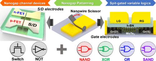
Nanogap engineering is developed for nanogap-induced field-effect transistors (FETs) and reconfigurable logic gates with ultrathin ambipolar 2H-MoTe2 channels. Via nanowire scissor technique, ∼50 nm nanogap channel FET and nanogap-driven spilt-gate (SG) FET are achieved at ease. Our 50 nm channel might be long for 4 nm-thin channel MoTe2, so that the short channel effect may be exempted; theoretical calculation results in a characteristic channel length λ of only 14 nm. However, it seems not long enough for a 12 nm-thick channel FET, which reveals visible short channel effects along with an increased λ (∼25 nm). It means that λ is not a strict standard, and much longer channel is necessary to practically prevent short channel effects. By the same nanogap technique, SG electrodes on a dielectric are fabricated to control the polarity of two separated channel locations. Reconfigurable functions are secured; NAND, OR, XOR, and SAND are nicely demonstrated by connecting two SG devices in series. These logic circuits are achieved with no change of device architecture but by properly arranging the connections and bias probing. Our nanogap device engineering is regarded as recommendable, showing its own benefits toward multifunctional devices, fabrication simplicity, and device architecture for the short channel study.
期刊介绍:
ACS Applied Electronic Materials is an interdisciplinary journal publishing original research covering all aspects of electronic materials. The journal is devoted to reports of new and original experimental and theoretical research of an applied nature that integrate knowledge in the areas of materials science, engineering, optics, physics, and chemistry into important applications of electronic materials. Sample research topics that span the journal's scope are inorganic, organic, ionic and polymeric materials with properties that include conducting, semiconducting, superconducting, insulating, dielectric, magnetic, optoelectronic, piezoelectric, ferroelectric and thermoelectric.
Indexed/Abstracted:
Web of Science SCIE
Scopus
CAS
INSPEC
Portico


 分享
分享
 求助内容:
求助内容: 应助结果提醒方式:
 扫码关注我们
