Alexandra Fonseca Montenegro, Marzieh Baan, Maryam Ghazisaeidi, Tyler J. Grassman and Roberto C. Myers*,
{"title":"Log-Normal Glide and the Formation of Misfit Dislocation Networks in Heteroepitaxial ZnS on GaP","authors":"Alexandra Fonseca Montenegro, Marzieh Baan, Maryam Ghazisaeidi, Tyler J. Grassman and Roberto C. Myers*, ","doi":"10.1021/acs.cgd.4c00559","DOIUrl":null,"url":null,"abstract":"<p >Scanning electron microscopy (SEM)-based electron channeling contrast imaging (ECCI) is used to observe and quantify misfit dislocation (MD) networks formed at the heteroepitaxial interface between ZnS and GaP grown by molecular beam epitaxy (MBE). Below a critical thickness of 15–20 nm, no MDs are observed. However, crystallographic features with strong dipole contrast, consistent with unexpanded dislocation half-loops, are observed prior to the formation of visible interfacial MD segments and any notable strain relaxation. At higher film thicknesses (20 to 50 nm), interfacial MD lengths increase anisotropically in the two orthogonal in-plane ⟨110⟩ line directions, threading dislocation (TD) density increases, and a roughening transition is observed from atomically smooth two-dimensional (2D) to a multistepped three-dimensional (3D) morphology, providing evidence for step edge pinning via surface terminating dislocations. The ZnS strain relaxation, calculated from the total MD content observed via ECCI, matches the average strain relaxation measured by high-resolution X-ray diffraction (HRXRD). The MD lengths are found to follow a log-normal distribution, indicating that the combined MD nucleation and TD glide processes must have a normal distribution of activation energies. The estimated TD glide velocity (<i>v</i><sub><i>g</i></sub>) along [<span>1</span>10] is almost twice that along [110], but in both directions shows a maximum as a function of film thickness, indicating an initial burst of plasticity followed by dislocation pinning.</p>","PeriodicalId":34,"journal":{"name":"Crystal Growth & Design","volume":"24 14","pages":"6007–6016"},"PeriodicalIF":3.4000,"publicationDate":"2024-07-03","publicationTypes":"Journal Article","fieldsOfStudy":null,"isOpenAccess":false,"openAccessPdf":"","citationCount":"0","resultStr":null,"platform":"Semanticscholar","paperid":null,"PeriodicalName":"Crystal Growth & Design","FirstCategoryId":"92","ListUrlMain":"https://pubs.acs.org/doi/10.1021/acs.cgd.4c00559","RegionNum":2,"RegionCategory":"化学","ArticlePicture":[],"TitleCN":null,"AbstractTextCN":null,"PMCID":null,"EPubDate":"","PubModel":"","JCR":"Q2","JCRName":"CHEMISTRY, MULTIDISCIPLINARY","Score":null,"Total":0}
引用次数: 0
Abstract
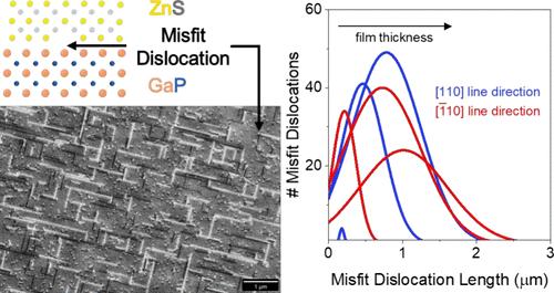
Scanning electron microscopy (SEM)-based electron channeling contrast imaging (ECCI) is used to observe and quantify misfit dislocation (MD) networks formed at the heteroepitaxial interface between ZnS and GaP grown by molecular beam epitaxy (MBE). Below a critical thickness of 15–20 nm, no MDs are observed. However, crystallographic features with strong dipole contrast, consistent with unexpanded dislocation half-loops, are observed prior to the formation of visible interfacial MD segments and any notable strain relaxation. At higher film thicknesses (20 to 50 nm), interfacial MD lengths increase anisotropically in the two orthogonal in-plane ⟨110⟩ line directions, threading dislocation (TD) density increases, and a roughening transition is observed from atomically smooth two-dimensional (2D) to a multistepped three-dimensional (3D) morphology, providing evidence for step edge pinning via surface terminating dislocations. The ZnS strain relaxation, calculated from the total MD content observed via ECCI, matches the average strain relaxation measured by high-resolution X-ray diffraction (HRXRD). The MD lengths are found to follow a log-normal distribution, indicating that the combined MD nucleation and TD glide processes must have a normal distribution of activation energies. The estimated TD glide velocity (vg) along [110] is almost twice that along [110], but in both directions shows a maximum as a function of film thickness, indicating an initial burst of plasticity followed by dislocation pinning.
期刊介绍:
The aim of Crystal Growth & Design is to stimulate crossfertilization of knowledge among scientists and engineers working in the fields of crystal growth, crystal engineering, and the industrial application of crystalline materials.
Crystal Growth & Design publishes theoretical and experimental studies of the physical, chemical, and biological phenomena and processes related to the design, growth, and application of crystalline materials. Synergistic approaches originating from different disciplines and technologies and integrating the fields of crystal growth, crystal engineering, intermolecular interactions, and industrial application are encouraged.


 分享
分享
 求助内容:
求助内容: 应助结果提醒方式:
 扫码关注我们
