Yingjie Tao, Ran Tian, Jiayuan Zhou, Kui Chu, Xuegang Chen, Wenshuai Gao, Guopeng Wang, Yuxuan Jiang, Kenji Watanabe, Takashi Taniguchi, Mingliang Tian, Xue Liu
{"title":"Optically Active Defect Engineering via Plasma Treatment in a MIS-Type 2D Heterostructure","authors":"Yingjie Tao, Ran Tian, Jiayuan Zhou, Kui Chu, Xuegang Chen, Wenshuai Gao, Guopeng Wang, Yuxuan Jiang, Kenji Watanabe, Takashi Taniguchi, Mingliang Tian, Xue Liu","doi":"10.1002/admi.202400288","DOIUrl":null,"url":null,"abstract":"<p>At the interface of 2D heterostructures, the presence of defects and their manipulation play a crucial role in the interfacial charge transfer behavior, further influencing the device functionality and performance. In this study, the impact of deliberately introduced photo-active defects in the h-BN layer on the interfacial charge transfer and photoresponse performance of a metal-insulator-semiconductor type heterostructure device is explored. The formation and concentration of defects are qualitatively controlled using an inductive coupled plasma treatment method, as evidenced by enhanced h-BN defect emission and more efficient optically induced doping of graphene at the graphene/h-BN interface. Besides, the use of the h-BN layer between graphene and WS<sub>2</sub> not only suppresses charge carriers in the dark state, but also promotes the separation of photo-generated electron-hole pairs and interfacial charge transfer due to the existence of defect levels, leading to orders of magnitude improvement in the light on/off ratio and self-driving performance of the heterostructure photodetector. This strategy of controlling defect states in the insulating layer provides a new approach to optimize the charge transfer processes at the 2D interfaces, so as to expand its potential applications in the fields of electronic and optoelectronic devices.</p>","PeriodicalId":115,"journal":{"name":"Advanced Materials Interfaces","volume":"11 29","pages":""},"PeriodicalIF":4.4000,"publicationDate":"2024-06-25","publicationTypes":"Journal Article","fieldsOfStudy":null,"isOpenAccess":false,"openAccessPdf":"https://onlinelibrary.wiley.com/doi/epdf/10.1002/admi.202400288","citationCount":"0","resultStr":null,"platform":"Semanticscholar","paperid":null,"PeriodicalName":"Advanced Materials Interfaces","FirstCategoryId":"88","ListUrlMain":"https://advanced.onlinelibrary.wiley.com/doi/10.1002/admi.202400288","RegionNum":3,"RegionCategory":"材料科学","ArticlePicture":[],"TitleCN":null,"AbstractTextCN":null,"PMCID":null,"EPubDate":"","PubModel":"","JCR":"Q2","JCRName":"CHEMISTRY, MULTIDISCIPLINARY","Score":null,"Total":0}
引用次数: 0
Abstract
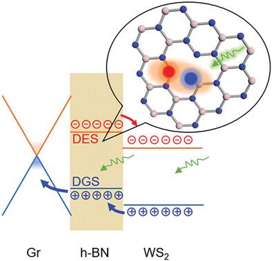
At the interface of 2D heterostructures, the presence of defects and their manipulation play a crucial role in the interfacial charge transfer behavior, further influencing the device functionality and performance. In this study, the impact of deliberately introduced photo-active defects in the h-BN layer on the interfacial charge transfer and photoresponse performance of a metal-insulator-semiconductor type heterostructure device is explored. The formation and concentration of defects are qualitatively controlled using an inductive coupled plasma treatment method, as evidenced by enhanced h-BN defect emission and more efficient optically induced doping of graphene at the graphene/h-BN interface. Besides, the use of the h-BN layer between graphene and WS2 not only suppresses charge carriers in the dark state, but also promotes the separation of photo-generated electron-hole pairs and interfacial charge transfer due to the existence of defect levels, leading to orders of magnitude improvement in the light on/off ratio and self-driving performance of the heterostructure photodetector. This strategy of controlling defect states in the insulating layer provides a new approach to optimize the charge transfer processes at the 2D interfaces, so as to expand its potential applications in the fields of electronic and optoelectronic devices.
期刊介绍:
Advanced Materials Interfaces publishes top-level research on interface technologies and effects. Considering any interface formed between solids, liquids, and gases, the journal ensures an interdisciplinary blend of physics, chemistry, materials science, and life sciences. Advanced Materials Interfaces was launched in 2014 and received an Impact Factor of 4.834 in 2018.
The scope of Advanced Materials Interfaces is dedicated to interfaces and surfaces that play an essential role in virtually all materials and devices. Physics, chemistry, materials science and life sciences blend to encourage new, cross-pollinating ideas, which will drive forward our understanding of the processes at the interface.
Advanced Materials Interfaces covers all topics in interface-related research:
Oil / water separation,
Applications of nanostructured materials,
2D materials and heterostructures,
Surfaces and interfaces in organic electronic devices,
Catalysis and membranes,
Self-assembly and nanopatterned surfaces,
Composite and coating materials,
Biointerfaces for technical and medical applications.
Advanced Materials Interfaces provides a forum for topics on surface and interface science with a wide choice of formats: Reviews, Full Papers, and Communications, as well as Progress Reports and Research News.


 分享
分享
 求助内容:
求助内容: 应助结果提醒方式:
 扫码关注我们
