Saravanan Yuvaraja, Hendrik Faber, Mritunjay Kumar, Na Xiao, Glen Isaac Maciel García, Xiao Tang, Thomas D. Anthopoulos, Xiaohang Li
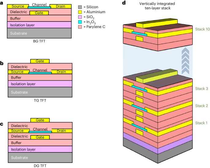
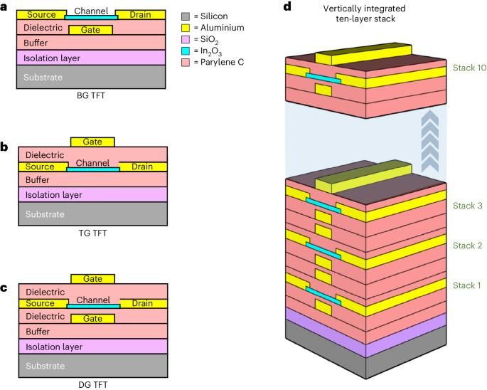
{"title":"Three-dimensional integrated metal-oxide transistors","authors":"Saravanan Yuvaraja, Hendrik Faber, Mritunjay Kumar, Na Xiao, Glen Isaac Maciel García, Xiao Tang, Thomas D. Anthopoulos, Xiaohang Li","doi":"10.1038/s41928-024-01205-0","DOIUrl":null,"url":null,"abstract":"The monolithic three-dimensional vertical integration of thin-film transistor (TFT) technologies could be used to create high-density, energy-efficient and low-cost integrated circuits. However, the development of scalable processes for integrating three-dimensional TFT devices is challenging. Here, we report the monolithic three-dimensional integration of indium oxide (In2O3) TFTs on a silicon/silicon dioxide (Si/SiO2) substrate at room temperature. We use an approach that is compatible with complementary metal–oxide–semiconductor (CMOS) processes to stack ten n-channel In2O3 TFTs. Different architectures—including bottom-, top- and dual-gate TFTs—can be fabricated at different layers in the stack. Our dual-gate devices exhibit enhanced electrical performance with a maximum field-effect mobility of 15 cm2 V−1 s−1, a subthreshold swing of 0.4 V dec−1 and a current on/off ratio of 108. By monolithically integrating dual-gate In2O3 TFTs at different locations in the stack, we created unipolar invertor circuits with a signal gain of around 50 and wide noise margins. The dual-gate devices also allow fine-tuning of the invertors to achieve symmetric voltage-transfer characteristics and optimal noise margins. A room-temperature approach to monolithic three-dimensional thin-film integration can be used to stack ten layers of n-channel indium oxide transistors on silicon/silicon dioxide substrates, while incorporating a range of architectures.","PeriodicalId":19064,"journal":{"name":"Nature Electronics","volume":"7 9","pages":"768-776"},"PeriodicalIF":40.9000,"publicationDate":"2024-07-08","publicationTypes":"Journal Article","fieldsOfStudy":null,"isOpenAccess":false,"openAccessPdf":"https://www.nature.com/articles/s41928-024-01205-0.pdf","citationCount":"0","resultStr":null,"platform":"Semanticscholar","paperid":null,"PeriodicalName":"Nature Electronics","FirstCategoryId":"5","ListUrlMain":"https://www.nature.com/articles/s41928-024-01205-0","RegionNum":1,"RegionCategory":"工程技术","ArticlePicture":[],"TitleCN":null,"AbstractTextCN":null,"PMCID":null,"EPubDate":"","PubModel":"","JCR":"Q1","JCRName":"ENGINEERING, ELECTRICAL & ELECTRONIC","Score":null,"Total":0}
引用次数: 0
Abstract
The monolithic three-dimensional vertical integration of thin-film transistor (TFT) technologies could be used to create high-density, energy-efficient and low-cost integrated circuits. However, the development of scalable processes for integrating three-dimensional TFT devices is challenging. Here, we report the monolithic three-dimensional integration of indium oxide (In2O3) TFTs on a silicon/silicon dioxide (Si/SiO2) substrate at room temperature. We use an approach that is compatible with complementary metal–oxide–semiconductor (CMOS) processes to stack ten n-channel In2O3 TFTs. Different architectures—including bottom-, top- and dual-gate TFTs—can be fabricated at different layers in the stack. Our dual-gate devices exhibit enhanced electrical performance with a maximum field-effect mobility of 15 cm2 V−1 s−1, a subthreshold swing of 0.4 V dec−1 and a current on/off ratio of 108. By monolithically integrating dual-gate In2O3 TFTs at different locations in the stack, we created unipolar invertor circuits with a signal gain of around 50 and wide noise margins. The dual-gate devices also allow fine-tuning of the invertors to achieve symmetric voltage-transfer characteristics and optimal noise margins. A room-temperature approach to monolithic three-dimensional thin-film integration can be used to stack ten layers of n-channel indium oxide transistors on silicon/silicon dioxide substrates, while incorporating a range of architectures.
期刊介绍:
Nature Electronics is a comprehensive journal that publishes both fundamental and applied research in the field of electronics. It encompasses a wide range of topics, including the study of new phenomena and devices, the design and construction of electronic circuits, and the practical applications of electronics. In addition, the journal explores the commercial and industrial aspects of electronics research.
The primary focus of Nature Electronics is on the development of technology and its potential impact on society. The journal incorporates the contributions of scientists, engineers, and industry professionals, offering a platform for their research findings. Moreover, Nature Electronics provides insightful commentary, thorough reviews, and analysis of the key issues that shape the field, as well as the technologies that are reshaping society.
Like all journals within the prestigious Nature brand, Nature Electronics upholds the highest standards of quality. It maintains a dedicated team of professional editors and follows a fair and rigorous peer-review process. The journal also ensures impeccable copy-editing and production, enabling swift publication. Additionally, Nature Electronics prides itself on its editorial independence, ensuring unbiased and impartial reporting.
In summary, Nature Electronics is a leading journal that publishes cutting-edge research in electronics. With its multidisciplinary approach and commitment to excellence, the journal serves as a valuable resource for scientists, engineers, and industry professionals seeking to stay at the forefront of advancements in the field.


 分享
分享
 求助内容:
求助内容: 应助结果提醒方式:
 扫码关注我们
