Modeling to study the shape, dimensionality and crystal structure dependence of energy band gap in nanosized semiconductors

IF 2.2 4区 工程技术 Q3 ENGINEERING, ELECTRICAL & ELECTRONIC Journal of Computational Electronics Pub Date : 2024-09-15 DOI:10.1007/s10825-024-02229-7
Monika Goyal
{"title":"Modeling to study the shape, dimensionality and crystal structure dependence of energy band gap in nanosized semiconductors","authors":"Monika Goyal","doi":"10.1007/s10825-024-02229-7","DOIUrl":null,"url":null,"abstract":"<div><p>In the present paper, a simple qualitative model is proposed to study the effect of dimension and crystal structure on the energy band gap of semiconducting nanomaterials. The energy band gap variation is studied for nanoparticles, nanowires and thin films. The model takes into account the crystal structure and to incorporate the effect of crystal structure on energy band gap, lattice packing fraction is included in the mathematical formulation. The model does not involve any approximation or adjustable parameter. The study on nanosized semiconductors is performed. The model results depict the increase in the energy bandgap of nanosized semiconductors with reduction in size to nanoscale. Based on dimensionality, increment in energy band gap of spherical nanoparticles (NP’s) is more than that in cylindrical nanowires (NW’s) and thin films. The model results are found in good agreement with compared experimental and stimulated data. Drastic increase in energy band gap in nano-semiconductor of diameter or height less than 10 nm is due to the quantum confinement of charge carriers with increase in the surface area/volume ratio. With reduction in size of the Nano semiconductor, increase in the Band gap is observed leading to the blue shift. The energy band gap dependence on size in the nanorange has opened the possibility of tuning the energy band gap of the nanomaterials and use them in the opto-electronic devices.</p></div>","PeriodicalId":620,"journal":{"name":"Journal of Computational Electronics","volume":"23 6","pages":"1284 - 1291"},"PeriodicalIF":2.2000,"publicationDate":"2024-09-15","publicationTypes":"Journal Article","fieldsOfStudy":null,"isOpenAccess":false,"openAccessPdf":"","citationCount":"0","resultStr":null,"platform":"Semanticscholar","paperid":null,"PeriodicalName":"Journal of Computational Electronics","FirstCategoryId":"5","ListUrlMain":"https://link.springer.com/article/10.1007/s10825-024-02229-7","RegionNum":4,"RegionCategory":"工程技术","ArticlePicture":[],"TitleCN":null,"AbstractTextCN":null,"PMCID":null,"EPubDate":"","PubModel":"","JCR":"Q3","JCRName":"ENGINEERING, ELECTRICAL & ELECTRONIC","Score":null,"Total":0}
引用次数: 0

Abstract

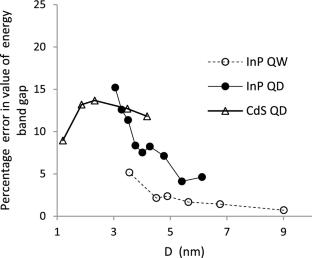
In the present paper, a simple qualitative model is proposed to study the effect of dimension and crystal structure on the energy band gap of semiconducting nanomaterials. The energy band gap variation is studied for nanoparticles, nanowires and thin films. The model takes into account the crystal structure and to incorporate the effect of crystal structure on energy band gap, lattice packing fraction is included in the mathematical formulation. The model does not involve any approximation or adjustable parameter. The study on nanosized semiconductors is performed. The model results depict the increase in the energy bandgap of nanosized semiconductors with reduction in size to nanoscale. Based on dimensionality, increment in energy band gap of spherical nanoparticles (NP’s) is more than that in cylindrical nanowires (NW’s) and thin films. The model results are found in good agreement with compared experimental and stimulated data. Drastic increase in energy band gap in nano-semiconductor of diameter or height less than 10 nm is due to the quantum confinement of charge carriers with increase in the surface area/volume ratio. With reduction in size of the Nano semiconductor, increase in the Band gap is observed leading to the blue shift. The energy band gap dependence on size in the nanorange has opened the possibility of tuning the energy band gap of the nanomaterials and use them in the opto-electronic devices.

Abstract Image

Abstract Image

查看原文
分享 分享
微信好友 朋友圈 QQ好友 复制链接
本刊更多论文
建模研究纳米级半导体能带隙的形状、尺寸和晶体结构相关性
本文提出了一个简单的定性模型来研究尺寸和晶体结构对半导体纳米材料能带隙的影响。研究了纳米颗粒、纳米线和薄膜的能带间隙变化。该模型考虑了晶体结构,并将晶体结构对能带隙的影响、晶格堆积分数纳入数学公式。该模型不涉及任何近似或可调参数。对纳米级半导体进行了研究。模型结果表明,随着尺寸缩小到纳米级,纳米级半导体的能带隙会增大。根据尺寸,球形纳米粒子(NP)的能带隙增量大于圆柱形纳米线(NW)和薄膜。模型结果与对比的实验数据和激发数据十分吻合。直径或高度小于 10 纳米的纳米半导体能带隙的急剧增大是由于电荷载流子的量子束缚随着表面积/体积比的增大而增大。随着纳米半导体尺寸的减小,能带隙也随之增大,从而导致蓝移。能带间隙与纳米尺寸的关系为调整纳米材料的能带间隙并将其用于光电子器件提供了可能。
本文章由计算机程序翻译,如有差异,请以英文原文为准。
求助全文
约1分钟内获得全文 去求助
来源期刊
Journal of Computational Electronics
Journal of Computational Electronics ENGINEERING, ELECTRICAL & ELECTRONIC-PHYSICS, APPLIED
CiteScore
4.50
自引率
4.80%
发文量
142
审稿时长
>12 weeks
期刊介绍: he Journal of Computational Electronics brings together research on all aspects of modeling and simulation of modern electronics. This includes optical, electronic, mechanical, and quantum mechanical aspects, as well as research on the underlying mathematical algorithms and computational details. The related areas of energy conversion/storage and of molecular and biological systems, in which the thrust is on the charge transport, electronic, mechanical, and optical properties, are also covered. In particular, we encourage manuscripts dealing with device simulation; with optical and optoelectronic systems and photonics; with energy storage (e.g. batteries, fuel cells) and harvesting (e.g. photovoltaic), with simulation of circuits, VLSI layout, logic and architecture (based on, for example, CMOS devices, quantum-cellular automata, QBITs, or single-electron transistors); with electromagnetic simulations (such as microwave electronics and components); or with molecular and biological systems. However, in all these cases, the submitted manuscripts should explicitly address the electronic properties of the relevant systems, materials, or devices and/or present novel contributions to the physical models, computational strategies, or numerical algorithms.
期刊最新文献
Study of the ISO-FDTD algorithm for processing higher-order dielectric function in SF-FDTD UTC-PD's optoelectronic mixing principle and optimal working condition Low-profile MIMO antenna for sub-6G smartphone applications with minimal footprint: an SVM-guided approach Impact of in-plane electric field on the optical properties of CO2 adsorbed 2D MoSe2 monolayer: application as a photodetector Empirical mathematical model based on optimized parameter extraction from captured electrohydrodynamic inkjet memristor device with LTspice model
×
引用
GB/T 7714-2015
复制
MLA
复制
APA
复制
导出至
BibTeX EndNote RefMan NoteFirst NoteExpress
×
×
提示
您的信息不完整,为了账户安全,请先补充。
现在去补充
×
提示
您因"违规操作"
具体请查看互助需知
我知道了
×
提示
现在去查看 取消
×
提示
确定
0
微信
客服QQ
Book学术公众号 扫码关注我们
反馈
×
意见反馈
请填写您的意见或建议
请填写您的手机或邮箱
已复制链接
已复制链接
快去分享给好友吧!
我知道了
×
扫码分享
扫码分享
Book学术官方微信
Book学术文献互助
Book学术文献互助群
群 号:481959085
Book学术
文献互助 智能选刊 最新文献 互助须知 联系我们:info@booksci.cn
Book学术提供免费学术资源搜索服务,方便国内外学者检索中英文文献。致力于提供最便捷和优质的服务体验。
Copyright © 2023 Book学术 All rights reserved.
ghs 京公网安备 11010802042870号 京ICP备2023020795号-1