{"title":"Metallurgical reactions and high-temperature long-term reliability of the Sn-2.3Ag flip-chip solder bump","authors":"Eun-Su Jang, Jeong-Won Yoon","doi":"10.1016/j.mee.2024.112293","DOIUrl":null,"url":null,"abstract":"<div><div>Flip-chip bonding technology has been extensively applied in the semiconductor packaging field given the recent increase in demand for electronic products requiring miniaturization and high performance. In this study, a high-temperature long-term reliability evaluation was performed to evaluate the metallurgical reaction and mechanical properties at the Sn-2.3Ag (wt%) flip-chip solder bump joints. Isothermal aging was performed for up to 2000 h at 150 °C. A Ni<sub>3</sub>Sn<sub>4</sub> intermetallic compound (IMC) was formed at the interface of the solder joints, and the thickness of the IMC layer increased as the isothermal aging time increased; however, the thickness of Ni under bump metallization (Ni UBM) layer was decreased during the growth of the IMC. Linear regression analysis showed that the growth thickness of the IMC layer and the consumption thickness of the Ni UBM layer varied linearly as functions of the square root of the isothermal aging time. Based on this analysis, the growth rate constant of the IMC layer and consumption rate constant of the Ni UBM layer were 0.000756 and 0.000303 μm/s<sup>1/2</sup>, respectively. Thereafter, shear tests were performed to evaluate the mechanical properties of the solder joints. As the isothermal aging time increased, the variation of shear strength was not large. However, the shear strength decreased slightly and then remained constant. As a result of the analysis of the fractured surface, most conditions exhibited ductile fracture behavior inside the solder bump, while in the case of specimens isothermally aged for 500, 1000, 1500, and 2000 h, cratering occurred. By observing the changes in the fracture mode, the ductile fracture behavior became less prominent, and the occurrence of cratering tended to become more prominent as the isothermal aging time increased.</div></div>","PeriodicalId":18557,"journal":{"name":"Microelectronic Engineering","volume":"296 ","pages":"Article 112293"},"PeriodicalIF":3.1000,"publicationDate":"2025-01-11","publicationTypes":"Journal Article","fieldsOfStudy":null,"isOpenAccess":false,"openAccessPdf":"","citationCount":"0","resultStr":null,"platform":"Semanticscholar","paperid":null,"PeriodicalName":"Microelectronic Engineering","FirstCategoryId":"5","ListUrlMain":"https://www.sciencedirect.com/science/article/pii/S016793172400162X","RegionNum":4,"RegionCategory":"工程技术","ArticlePicture":[],"TitleCN":null,"AbstractTextCN":null,"PMCID":null,"EPubDate":"2024/11/29 0:00:00","PubModel":"Epub","JCR":"Q2","JCRName":"ENGINEERING, ELECTRICAL & ELECTRONIC","Score":null,"Total":0}
引用次数: 0
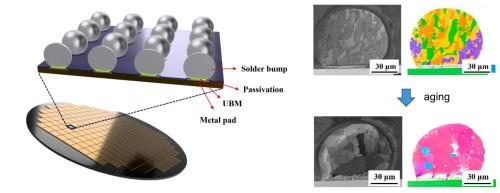
Abstract
Flip-chip bonding technology has been extensively applied in the semiconductor packaging field given the recent increase in demand for electronic products requiring miniaturization and high performance. In this study, a high-temperature long-term reliability evaluation was performed to evaluate the metallurgical reaction and mechanical properties at the Sn-2.3Ag (wt%) flip-chip solder bump joints. Isothermal aging was performed for up to 2000 h at 150 °C. A Ni3Sn4 intermetallic compound (IMC) was formed at the interface of the solder joints, and the thickness of the IMC layer increased as the isothermal aging time increased; however, the thickness of Ni under bump metallization (Ni UBM) layer was decreased during the growth of the IMC. Linear regression analysis showed that the growth thickness of the IMC layer and the consumption thickness of the Ni UBM layer varied linearly as functions of the square root of the isothermal aging time. Based on this analysis, the growth rate constant of the IMC layer and consumption rate constant of the Ni UBM layer were 0.000756 and 0.000303 μm/s1/2, respectively. Thereafter, shear tests were performed to evaluate the mechanical properties of the solder joints. As the isothermal aging time increased, the variation of shear strength was not large. However, the shear strength decreased slightly and then remained constant. As a result of the analysis of the fractured surface, most conditions exhibited ductile fracture behavior inside the solder bump, while in the case of specimens isothermally aged for 500, 1000, 1500, and 2000 h, cratering occurred. By observing the changes in the fracture mode, the ductile fracture behavior became less prominent, and the occurrence of cratering tended to become more prominent as the isothermal aging time increased.
期刊介绍:
Microelectronic Engineering is the premier nanoprocessing, and nanotechnology journal focusing on fabrication of electronic, photonic, bioelectronic, electromechanic and fluidic devices and systems, and their applications in the broad areas of electronics, photonics, energy, life sciences, and environment. It covers also the expanding interdisciplinary field of "more than Moore" and "beyond Moore" integrated nanoelectronics / photonics and micro-/nano-/bio-systems. Through its unique mixture of peer-reviewed articles, reviews, accelerated publications, short and Technical notes, and the latest research news on key developments, Microelectronic Engineering provides comprehensive coverage of this exciting, interdisciplinary and dynamic new field for researchers in academia and professionals in industry.


 分享
分享
 求助内容:
求助内容: 应助结果提醒方式:
 扫码关注我们
