Jiangxia Huang, Wenxin Lin, Shuxin Li, Jiahao Li, Haonan Feng, Xiongfeng Lin, Yulin Guo, Wenlin Liang, Longjia Wu, Paul W. M. Blom, Quan Niu, Yuguang Ma
{"title":"Hole Trap Formation in Quantum Dot Light-Emitting Diodes Under Electrical Stress","authors":"Jiangxia Huang, Wenxin Lin, Shuxin Li, Jiahao Li, Haonan Feng, Xiongfeng Lin, Yulin Guo, Wenlin Liang, Longjia Wu, Paul W. M. Blom, Quan Niu, Yuguang Ma","doi":"10.1002/aelm.202400231","DOIUrl":null,"url":null,"abstract":"<p>Quantum dot light-emitting diodes (QLEDs) have emerged as promising candidates for next-generation display technology, but the limited lifetime of QLEDs hampers their further commercialization. Despite extensive research that has been conducted for the last decades, the mechanism leading to the rapid degradation of QLEDs remains unclear. Here, the formation of hole traps is demonstrated as the critical reason for the degradation of QLEDs. Applying impedance measurements, an enhancement of the negative capacitance is observed and provides straightforward evidence for the formation of hole traps. The generated hole traps introduce additional trap-assisted recombination of trapped holes with free electrons, as reflected by the evolution and voltage dependence of the electroluminescence spectra, leading to efficiency loss in degraded devices. By performing numerical simulations to model the degradation of QLEDs, the formation of hole traps is quantified as a function of aging time. The calculated hole trap density is consistent with that as measured from impedance spectroscopy, validating that the hole trap formation is the mechanism for the voltage drift and efficiency decrease of QLEDs under constant current stress.</p>","PeriodicalId":110,"journal":{"name":"Advanced Electronic Materials","volume":"11 3","pages":""},"PeriodicalIF":5.3000,"publicationDate":"2024-12-20","publicationTypes":"Journal Article","fieldsOfStudy":null,"isOpenAccess":false,"openAccessPdf":"https://onlinelibrary.wiley.com/doi/epdf/10.1002/aelm.202400231","citationCount":"0","resultStr":null,"platform":"Semanticscholar","paperid":null,"PeriodicalName":"Advanced Electronic Materials","FirstCategoryId":"88","ListUrlMain":"https://advanced.onlinelibrary.wiley.com/doi/10.1002/aelm.202400231","RegionNum":2,"RegionCategory":"材料科学","ArticlePicture":[],"TitleCN":null,"AbstractTextCN":null,"PMCID":null,"EPubDate":"","PubModel":"","JCR":"Q2","JCRName":"MATERIALS SCIENCE, MULTIDISCIPLINARY","Score":null,"Total":0}
引用次数: 0
Abstract
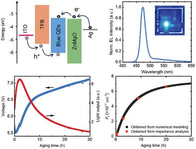
Quantum dot light-emitting diodes (QLEDs) have emerged as promising candidates for next-generation display technology, but the limited lifetime of QLEDs hampers their further commercialization. Despite extensive research that has been conducted for the last decades, the mechanism leading to the rapid degradation of QLEDs remains unclear. Here, the formation of hole traps is demonstrated as the critical reason for the degradation of QLEDs. Applying impedance measurements, an enhancement of the negative capacitance is observed and provides straightforward evidence for the formation of hole traps. The generated hole traps introduce additional trap-assisted recombination of trapped holes with free electrons, as reflected by the evolution and voltage dependence of the electroluminescence spectra, leading to efficiency loss in degraded devices. By performing numerical simulations to model the degradation of QLEDs, the formation of hole traps is quantified as a function of aging time. The calculated hole trap density is consistent with that as measured from impedance spectroscopy, validating that the hole trap formation is the mechanism for the voltage drift and efficiency decrease of QLEDs under constant current stress.
期刊介绍:
Advanced Electronic Materials is an interdisciplinary forum for peer-reviewed, high-quality, high-impact research in the fields of materials science, physics, and engineering of electronic and magnetic materials. It includes research on physics and physical properties of electronic and magnetic materials, spintronics, electronics, device physics and engineering, micro- and nano-electromechanical systems, and organic electronics, in addition to fundamental research.


 分享
分享
 求助内容:
求助内容: 应助结果提醒方式:
 扫码关注我们
