Viswanath G. Akkili, Jongchan Yoon, Kihyun Shin, Sanghyun Jeong, Ji-Yun Moon, Jun-Hui Choi, Seung-Il Kim, Ashish A. Patil, Frederick Aziadzo, Jeongbeen Kim, Suhyeon Kim, Dong-Wook Shin, Jung-Sub Wi, Hoon-Hwe Cho, Joon Sik Park, Eui-Tae Kim, Dong-Eun Kim, Jaeyeong Heo, Graeme Henkelman, Kostya S. Novoselov, Choong-Heui Chung, Jae-Hyun Lee, Zonghoon Lee, Sangyeob Lee
{"title":"Amorphous Carbon Monolayer: A van der Waals Interface for High-Performance Metal Oxide Semiconductor Devices","authors":"Viswanath G. Akkili, Jongchan Yoon, Kihyun Shin, Sanghyun Jeong, Ji-Yun Moon, Jun-Hui Choi, Seung-Il Kim, Ashish A. Patil, Frederick Aziadzo, Jeongbeen Kim, Suhyeon Kim, Dong-Wook Shin, Jung-Sub Wi, Hoon-Hwe Cho, Joon Sik Park, Eui-Tae Kim, Dong-Eun Kim, Jaeyeong Heo, Graeme Henkelman, Kostya S. Novoselov, Choong-Heui Chung, Jae-Hyun Lee, Zonghoon Lee, Sangyeob Lee","doi":"10.1021/acsnano.4c12780","DOIUrl":null,"url":null,"abstract":"Ultrasmall-scale semiconductor devices (≤5 nm) are advancing technologies, such as artificial intelligence and the Internet of Things. However, the further scaling of these devices poses critical challenges, such as interface properties and oxide quality, particularly at the high-<i>k</i>/semiconductor interface in metal-oxide-semiconductor (MOS) devices. Existing interlayer (IL) methods, typically exceeding 1 nm thickness, are unsuitable for ultrasmall-scale devices. Here, we propose a one-atom-thick amorphous carbon monolayer (ACM) as the IL to address these issues for MOS devices. ACM is disordered, randomly arranged, and short of long-range periodicity with <i>sp</i><sup>2</sup> hybridized carbon network, offering impermeability, van der Waals (vdW) bonding, insulating behavior, and effective seeding layer. With these advantages, we have utilized ACM vdW IL (vIL) in Al<sub>2</sub>O<sub>3</sub>/H–Ge MOS capacitors. The interface trap density was suppressed by ∼2 orders of magnitude to 7.21 × 10<sup>10</sup> cm<sup>–2</sup> eV<sup>–1</sup>, with no frequency-dependent flat band shift. The slow trap density is decreased to 2 orders of magnitude, and the <i>C</i>–<i>V</i> hysteresis width is minimized by >75%, indicating enhanced oxide quality. These results are supported by high-resolution transmission electron microscopy and energy dispersive X-ray spectroscopy analysis, confirming the creation of an atomically well-defined interface in the Al<sub>2</sub>O<sub>3</sub>/H–Ge heterojunction with ACM vIL, even under high-temperature annealing conditions. Density functional theory calculations further clarify that ACM vIL preserves the hydrogen-passivated Ge surface without altering its electronic band structure. These results demonstrate that ACM vIL effectively improves the interface properties and enhances the oxide quality, enabling further advancements in ultrasmall-scale MOS devices.","PeriodicalId":21,"journal":{"name":"ACS Nano","volume":"54 1","pages":""},"PeriodicalIF":16.0000,"publicationDate":"2024-12-31","publicationTypes":"Journal Article","fieldsOfStudy":null,"isOpenAccess":false,"openAccessPdf":"","citationCount":"0","resultStr":null,"platform":"Semanticscholar","paperid":null,"PeriodicalName":"ACS Nano","FirstCategoryId":"88","ListUrlMain":"https://doi.org/10.1021/acsnano.4c12780","RegionNum":1,"RegionCategory":"材料科学","ArticlePicture":[],"TitleCN":null,"AbstractTextCN":null,"PMCID":null,"EPubDate":"","PubModel":"","JCR":"Q1","JCRName":"CHEMISTRY, MULTIDISCIPLINARY","Score":null,"Total":0}
引用次数: 0
Abstract
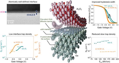
Ultrasmall-scale semiconductor devices (≤5 nm) are advancing technologies, such as artificial intelligence and the Internet of Things. However, the further scaling of these devices poses critical challenges, such as interface properties and oxide quality, particularly at the high-k/semiconductor interface in metal-oxide-semiconductor (MOS) devices. Existing interlayer (IL) methods, typically exceeding 1 nm thickness, are unsuitable for ultrasmall-scale devices. Here, we propose a one-atom-thick amorphous carbon monolayer (ACM) as the IL to address these issues for MOS devices. ACM is disordered, randomly arranged, and short of long-range periodicity with sp2 hybridized carbon network, offering impermeability, van der Waals (vdW) bonding, insulating behavior, and effective seeding layer. With these advantages, we have utilized ACM vdW IL (vIL) in Al2O3/H–Ge MOS capacitors. The interface trap density was suppressed by ∼2 orders of magnitude to 7.21 × 1010 cm–2 eV–1, with no frequency-dependent flat band shift. The slow trap density is decreased to 2 orders of magnitude, and the C–V hysteresis width is minimized by >75%, indicating enhanced oxide quality. These results are supported by high-resolution transmission electron microscopy and energy dispersive X-ray spectroscopy analysis, confirming the creation of an atomically well-defined interface in the Al2O3/H–Ge heterojunction with ACM vIL, even under high-temperature annealing conditions. Density functional theory calculations further clarify that ACM vIL preserves the hydrogen-passivated Ge surface without altering its electronic band structure. These results demonstrate that ACM vIL effectively improves the interface properties and enhances the oxide quality, enabling further advancements in ultrasmall-scale MOS devices.
期刊介绍:
ACS Nano, published monthly, serves as an international forum for comprehensive articles on nanoscience and nanotechnology research at the intersections of chemistry, biology, materials science, physics, and engineering. The journal fosters communication among scientists in these communities, facilitating collaboration, new research opportunities, and advancements through discoveries. ACS Nano covers synthesis, assembly, characterization, theory, and simulation of nanostructures, nanobiotechnology, nanofabrication, methods and tools for nanoscience and nanotechnology, and self- and directed-assembly. Alongside original research articles, it offers thorough reviews, perspectives on cutting-edge research, and discussions envisioning the future of nanoscience and nanotechnology.


 分享
分享
 求助内容:
求助内容: 应助结果提醒方式:
 扫码关注我们
