Chun-Sheng Jiang, Rouin Farshchi, Timothy Nagle, Dingyuan Lu, Gang Xiong, Lorelle M Mansfield, Matthew O Reese
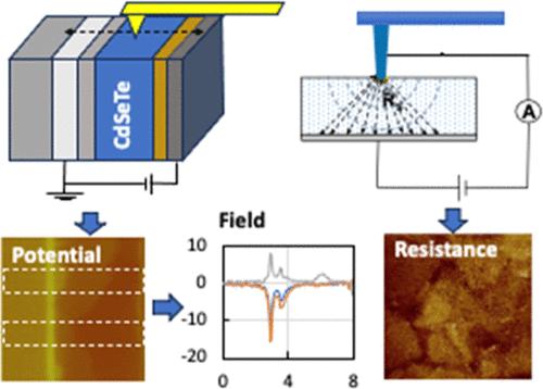
{"title":"Microelectronic Structure and Doping Nonuniformity of Phosphorus-Doped CdSeTe Solar Cells.","authors":"Chun-Sheng Jiang, Rouin Farshchi, Timothy Nagle, Dingyuan Lu, Gang Xiong, Lorelle M Mansfield, Matthew O Reese","doi":"10.1021/acsami.4c15741","DOIUrl":null,"url":null,"abstract":"<p><p>Optimizing group-V doping and Se alloying are two main focuses for advancing CdTe photovoltaic technology. We report on nanometer-scale characterizations of microelectronic structures of phosphorus (P)-doped CdSeTe devices using a combination of two atomic force microscopy-based techniques, namely, Kelvin probe force microscopy (KPFM) and scanning spreading resistance microscopy (SSRM). KPFM on device cross-section images distribution of the potential drop across the device. SSRM taken on a delaminated front interface and further beveling into absorber bulk reveals local distributions of doping polarity and carrier concentration. The KPFM and SSRM imaging corroborate each other, suggesting that nonuniform doping revealed by SSRM is associated with nonuniform potential features observed by KPFM. These detrimental microelectronic structures were improved by enhancing P-doping. The large nonuniform potential drop and deep overall n-p transition in the device without doping were mitigated to potential fluctuation around the front interface and n-p transition depth of ∼100 nm by low-level P-doping and further mitigated to scarce and slight irregular potential and p-weighed doping at the interface by high-level P-doping. These characterizations imply sophisticated defect chemistry, atomic structure, and associated electronic structure in CdTe with Se alloying and group-V doping together and further point to the direction for improving device efficiency by mitigating and ultimately eliminating the nonuniform doping and irregular potential.</p>","PeriodicalId":5,"journal":{"name":"ACS Applied Materials & Interfaces","volume":" ","pages":"3278-3288"},"PeriodicalIF":8.2000,"publicationDate":"2025-01-15","publicationTypes":"Journal Article","fieldsOfStudy":null,"isOpenAccess":false,"openAccessPdf":"https://www.ncbi.nlm.nih.gov/pmc/articles/PMC11744667/pdf/","citationCount":"0","resultStr":null,"platform":"Semanticscholar","paperid":null,"PeriodicalName":"ACS Applied Materials & Interfaces","FirstCategoryId":"88","ListUrlMain":"https://doi.org/10.1021/acsami.4c15741","RegionNum":2,"RegionCategory":"材料科学","ArticlePicture":[],"TitleCN":null,"AbstractTextCN":null,"PMCID":null,"EPubDate":"2025/1/6 0:00:00","PubModel":"Epub","JCR":"Q1","JCRName":"MATERIALS SCIENCE, MULTIDISCIPLINARY","Score":null,"Total":0}
引用次数: 0
Abstract
Optimizing group-V doping and Se alloying are two main focuses for advancing CdTe photovoltaic technology. We report on nanometer-scale characterizations of microelectronic structures of phosphorus (P)-doped CdSeTe devices using a combination of two atomic force microscopy-based techniques, namely, Kelvin probe force microscopy (KPFM) and scanning spreading resistance microscopy (SSRM). KPFM on device cross-section images distribution of the potential drop across the device. SSRM taken on a delaminated front interface and further beveling into absorber bulk reveals local distributions of doping polarity and carrier concentration. The KPFM and SSRM imaging corroborate each other, suggesting that nonuniform doping revealed by SSRM is associated with nonuniform potential features observed by KPFM. These detrimental microelectronic structures were improved by enhancing P-doping. The large nonuniform potential drop and deep overall n-p transition in the device without doping were mitigated to potential fluctuation around the front interface and n-p transition depth of ∼100 nm by low-level P-doping and further mitigated to scarce and slight irregular potential and p-weighed doping at the interface by high-level P-doping. These characterizations imply sophisticated defect chemistry, atomic structure, and associated electronic structure in CdTe with Se alloying and group-V doping together and further point to the direction for improving device efficiency by mitigating and ultimately eliminating the nonuniform doping and irregular potential.
优化 V 族掺杂和硒合金化是推动碲化镉光伏技术发展的两大重点。我们结合两种基于原子力显微镜的技术,即开尔文探针力显微镜(KPFM)和扫描展阻显微镜(SSRM),报告了掺磷(P)碲化镉器件微电子结构的纳米级表征。开尔文探针力显微镜在器件横截面上拍摄的图像显示了器件上的电位降分布。SSRM 在分层的前界面上拍摄,并进一步斜切到吸收器体,显示了掺杂极性和载流子浓度的局部分布。KPFM 和 SSRM 成像相互印证,表明 SSRM 揭示的非均匀掺杂与 KPFM 观察到的非均匀电位特征有关。通过加强 P 掺杂,这些有害的微电子结构得到了改善。通过低级 P 掺杂,未掺杂器件中的大量不均匀电位下降和整体深度 n-p 转变被缓解为前界面周围的电位波动和 ∼100 nm 的 n-p 转变深度;通过高级 P 掺杂,进一步缓解为界面上稀少的轻微不规则电位和 p 权衡掺杂。这些表征意味着碲化镉在硒合金化和 V 族掺杂的作用下具有复杂的缺陷化学、原子结构和相关电子结构,并进一步指明了通过减轻并最终消除不均匀掺杂和不规则电位来提高器件效率的方向。
期刊介绍:
ACS Applied Materials & Interfaces is a leading interdisciplinary journal that brings together chemists, engineers, physicists, and biologists to explore the development and utilization of newly-discovered materials and interfacial processes for specific applications. Our journal has experienced remarkable growth since its establishment in 2009, both in terms of the number of articles published and the impact of the research showcased. We are proud to foster a truly global community, with the majority of published articles originating from outside the United States, reflecting the rapid growth of applied research worldwide.


 分享
分享
 求助内容:
求助内容: 应助结果提醒方式:
 扫码关注我们
