Goeun Pyo, Su Jin Heo, Dongsu Kim, Minji Yu, Joonghyun Kim, SeungNam Cha, Hyuk-Jun Kwon, Jae Eun Jang
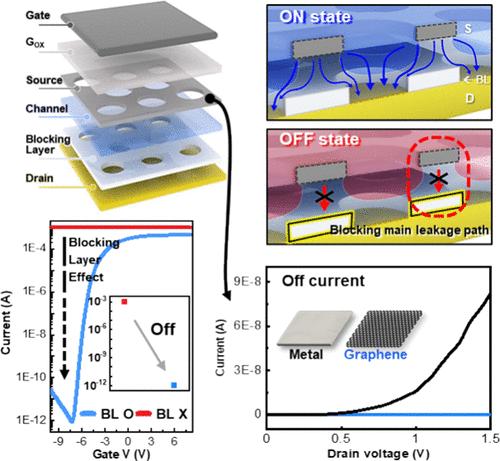
{"title":"Study of High Performance Nanoscale Channel Length Vertical Transistors with a Self-Aligned Blocking Layer.","authors":"Goeun Pyo, Su Jin Heo, Dongsu Kim, Minji Yu, Joonghyun Kim, SeungNam Cha, Hyuk-Jun Kwon, Jae Eun Jang","doi":"10.1021/acsami.4c16429","DOIUrl":null,"url":null,"abstract":"<p><p>A transistor design employing all vertically stacked components has attracted considerable attention due to the simplicity of the fabrication process and the high conductivity easily realized by achieving nanolevel short channel lengths with two-dimensional current paths. However, fundamental issues, specifically the blocking of the gate electrical field to the semiconductive channel layer and high leakage current at the \"off\" state, have impeded this configuration in becoming a major transistor design. To address these issues, it has been proposed to introduce a blocking layer (BL) with embedded hole structures and source electrode with embedded hole structures, enhancing gate field penetration and carrier modulation. The hole structure embedded in the source and the BL on the drain induced a desirable combined effect of gate field penetration and carrier pathway modulation. The align accuracy and the hole size difference between BL and source electrode were confirmed as the most important design parameters for high performance of a transistor. We therefore proposed a self-aligning lithography method using a built-in mask that allows high alignment accuracy between the source hole structure and the BL hole structure on the drain over a large area without a high-resolution process system. This method also enables easy and fast fabrication of nanoscale channels with high performance. This design resulted in a transistor with an output of 28 mA/cm<sup>2</sup> and an on-off ratio exceeding 10<sup>6</sup> at 1 mV of <i>V</i><sub>DS</sub>. However, at 3 V of <i>V</i><sub>DS</sub>, the off-current increased significantly due to short-channel effects in the all metal electrode design. To solve this issue, Fermi level-tunable graphene replaced metal electrodes, maintaining an off-current below 10 pA and an on-off ratio around 10<sup>7</sup> at 3 V. In addition, the device demonstrates robust electrical properties to light without any special treatment and is stable with a threshold voltage shift of less than 1 V under bias stress. This study demonstrates that the proposed vertical transistor design is a viable candidate as a new major transistor design for various applications.</p>","PeriodicalId":5,"journal":{"name":"ACS Applied Materials & Interfaces","volume":" ","pages":"8474-8484"},"PeriodicalIF":8.2000,"publicationDate":"2025-02-05","publicationTypes":"Journal Article","fieldsOfStudy":null,"isOpenAccess":false,"openAccessPdf":"","citationCount":"0","resultStr":null,"platform":"Semanticscholar","paperid":null,"PeriodicalName":"ACS Applied Materials & Interfaces","FirstCategoryId":"88","ListUrlMain":"https://doi.org/10.1021/acsami.4c16429","RegionNum":2,"RegionCategory":"材料科学","ArticlePicture":[],"TitleCN":null,"AbstractTextCN":null,"PMCID":null,"EPubDate":"2025/1/21 0:00:00","PubModel":"Epub","JCR":"Q1","JCRName":"MATERIALS SCIENCE, MULTIDISCIPLINARY","Score":null,"Total":0}
引用次数: 0
Abstract
A transistor design employing all vertically stacked components has attracted considerable attention due to the simplicity of the fabrication process and the high conductivity easily realized by achieving nanolevel short channel lengths with two-dimensional current paths. However, fundamental issues, specifically the blocking of the gate electrical field to the semiconductive channel layer and high leakage current at the "off" state, have impeded this configuration in becoming a major transistor design. To address these issues, it has been proposed to introduce a blocking layer (BL) with embedded hole structures and source electrode with embedded hole structures, enhancing gate field penetration and carrier modulation. The hole structure embedded in the source and the BL on the drain induced a desirable combined effect of gate field penetration and carrier pathway modulation. The align accuracy and the hole size difference between BL and source electrode were confirmed as the most important design parameters for high performance of a transistor. We therefore proposed a self-aligning lithography method using a built-in mask that allows high alignment accuracy between the source hole structure and the BL hole structure on the drain over a large area without a high-resolution process system. This method also enables easy and fast fabrication of nanoscale channels with high performance. This design resulted in a transistor with an output of 28 mA/cm2 and an on-off ratio exceeding 106 at 1 mV of VDS. However, at 3 V of VDS, the off-current increased significantly due to short-channel effects in the all metal electrode design. To solve this issue, Fermi level-tunable graphene replaced metal electrodes, maintaining an off-current below 10 pA and an on-off ratio around 107 at 3 V. In addition, the device demonstrates robust electrical properties to light without any special treatment and is stable with a threshold voltage shift of less than 1 V under bias stress. This study demonstrates that the proposed vertical transistor design is a viable candidate as a new major transistor design for various applications.
期刊介绍:
ACS Applied Materials & Interfaces is a leading interdisciplinary journal that brings together chemists, engineers, physicists, and biologists to explore the development and utilization of newly-discovered materials and interfacial processes for specific applications. Our journal has experienced remarkable growth since its establishment in 2009, both in terms of the number of articles published and the impact of the research showcased. We are proud to foster a truly global community, with the majority of published articles originating from outside the United States, reflecting the rapid growth of applied research worldwide.


 分享
分享
 求助内容:
求助内容: 应助结果提醒方式:
 扫码关注我们
