Jung-Soo Ko, Sol Lee, Robert K. A. Bennett, Kirstin Schauble, Marc Jaikissoon, Kathryn Neilson, Anh Tuan Hoang, Andrew J. Mannix, Kwanpyo Kim, Krishna C. Saraswat, Eric Pop
{"title":"Sub-Nanometer Equivalent Oxide Thickness and Threshold Voltage Control Enabled by Silicon Seed Layer on Monolayer MoS2 Transistors","authors":"Jung-Soo Ko, Sol Lee, Robert K. A. Bennett, Kirstin Schauble, Marc Jaikissoon, Kathryn Neilson, Anh Tuan Hoang, Andrew J. Mannix, Kwanpyo Kim, Krishna C. Saraswat, Eric Pop","doi":"10.1021/acs.nanolett.4c01775","DOIUrl":null,"url":null,"abstract":"Low-power transistors based on two-dimensional (2D) semiconductors require ultrathin gate insulators, whose atomic layer deposition (ALD) has been difficult without adequate surface preparation. Here, we achieve sub-1 nm equivalent oxide thickness (EOT) on monolayer MoS<sub>2</sub> using HfO<sub>2</sub> and a simple, commonly available Si seed. We first investigate six seed layer candidates (Si, Ge, Hf, La, Gd, Al<sub>2</sub>O<sub>3</sub>) and find that only Si and Ge cause no measurable damage to the MoS<sub>2</sub>. With these, we build monolayer MoS<sub>2</sub> transistors using ALD of HfO<sub>2</sub> top-gate dielectric and find that the Si seed provides the better, low-hysteresis interface. The thickness of this interfacial layer also controls the threshold voltage, enabling normally-off, well-behaved transistors. The thinnest gate stack reached low EOT ≈ 0.9 nm with low leakage (<0.6 μA/cm<sup>2</sup>) and ∼80 mV/dec subthreshold swing at room temperature. This represents a simple top-gate dielectric deposition approach, achievable within many common nanofabrication facilities.","PeriodicalId":53,"journal":{"name":"Nano Letters","volume":"77 1","pages":""},"PeriodicalIF":9.1000,"publicationDate":"2025-02-04","publicationTypes":"Journal Article","fieldsOfStudy":null,"isOpenAccess":false,"openAccessPdf":"","citationCount":"0","resultStr":null,"platform":"Semanticscholar","paperid":null,"PeriodicalName":"Nano Letters","FirstCategoryId":"88","ListUrlMain":"https://doi.org/10.1021/acs.nanolett.4c01775","RegionNum":1,"RegionCategory":"材料科学","ArticlePicture":[],"TitleCN":null,"AbstractTextCN":null,"PMCID":null,"EPubDate":"","PubModel":"","JCR":"Q1","JCRName":"CHEMISTRY, MULTIDISCIPLINARY","Score":null,"Total":0}
引用次数: 0
Abstract
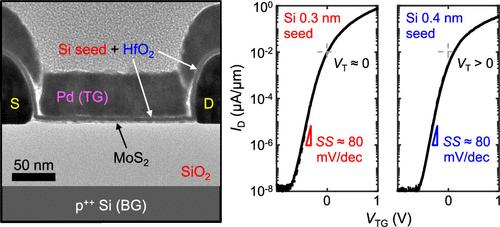
Low-power transistors based on two-dimensional (2D) semiconductors require ultrathin gate insulators, whose atomic layer deposition (ALD) has been difficult without adequate surface preparation. Here, we achieve sub-1 nm equivalent oxide thickness (EOT) on monolayer MoS2 using HfO2 and a simple, commonly available Si seed. We first investigate six seed layer candidates (Si, Ge, Hf, La, Gd, Al2O3) and find that only Si and Ge cause no measurable damage to the MoS2. With these, we build monolayer MoS2 transistors using ALD of HfO2 top-gate dielectric and find that the Si seed provides the better, low-hysteresis interface. The thickness of this interfacial layer also controls the threshold voltage, enabling normally-off, well-behaved transistors. The thinnest gate stack reached low EOT ≈ 0.9 nm with low leakage (<0.6 μA/cm2) and ∼80 mV/dec subthreshold swing at room temperature. This represents a simple top-gate dielectric deposition approach, achievable within many common nanofabrication facilities.
期刊介绍:
Nano Letters serves as a dynamic platform for promptly disseminating original results in fundamental, applied, and emerging research across all facets of nanoscience and nanotechnology. A pivotal criterion for inclusion within Nano Letters is the convergence of at least two different areas or disciplines, ensuring a rich interdisciplinary scope. The journal is dedicated to fostering exploration in diverse areas, including:
- Experimental and theoretical findings on physical, chemical, and biological phenomena at the nanoscale
- Synthesis, characterization, and processing of organic, inorganic, polymer, and hybrid nanomaterials through physical, chemical, and biological methodologies
- Modeling and simulation of synthetic, assembly, and interaction processes
- Realization of integrated nanostructures and nano-engineered devices exhibiting advanced performance
- Applications of nanoscale materials in living and environmental systems
Nano Letters is committed to advancing and showcasing groundbreaking research that intersects various domains, fostering innovation and collaboration in the ever-evolving field of nanoscience and nanotechnology.


 分享
分享
 求助内容:
求助内容: 应助结果提醒方式:
 扫码关注我们
