Sudipta Majumder, Sarika Lohkna, Vaibhav Walve, Rahul Chand, Gokul M. Anilkumar, Sooyeon Hwang, G. V. Pavan Kumar, Aparna Deshpande, Prasenjit Ghosh, Atikur Rahman
{"title":"Unveiling the Correlation between Defects and High Mobility in MoS2 Monolayers","authors":"Sudipta Majumder, Sarika Lohkna, Vaibhav Walve, Rahul Chand, Gokul M. Anilkumar, Sooyeon Hwang, G. V. Pavan Kumar, Aparna Deshpande, Prasenjit Ghosh, Atikur Rahman","doi":"10.1021/acsami.4c18552","DOIUrl":null,"url":null,"abstract":"Defects in semiconductors play a crucial role in modifying their electronic structure and transport properties. In transition metal dichalcogenides, atomic chalcogen vacancies are a primary source of intrinsic defects. While the impact of these vacancies on electrical transport has been widely studied, their exact role remains not fully understood. In this work, we correlate optical spectroscopy, low-temperature electrical transport measurements, scanning tunneling microscopy (STM), and first-principles density functional theory (DFT) calculations to explore the effect of chalcogen vacancies in MoS<sub>2</sub> monolayers grown by chemical vapor deposition. We specifically highlight the role of disulfur vacancies in modulating electrical properties, showing that these defects increase the density of shallow donor states near the conduction band, which facilitates electron hopping conduction, as evidenced by low-temperature transport and STM measurements. These findings are further supported by DFT calculations, which reveal that the electronic states associated with these defects are relatively delocalized, promoting hopping conduction and inducing n-type doping. This mechanism accounts for the observed high field-effect mobility (>100 cm<sup>2</sup> V<sup>–1</sup>s<sup>–1</sup>) in the samples. These findings highlight the potential for defect engineering as a universal approach to customizing the properties of 2D materials for various applications.","PeriodicalId":5,"journal":{"name":"ACS Applied Materials & Interfaces","volume":"36 1","pages":""},"PeriodicalIF":8.2000,"publicationDate":"2025-02-05","publicationTypes":"Journal Article","fieldsOfStudy":null,"isOpenAccess":false,"openAccessPdf":"","citationCount":"0","resultStr":null,"platform":"Semanticscholar","paperid":null,"PeriodicalName":"ACS Applied Materials & Interfaces","FirstCategoryId":"88","ListUrlMain":"https://doi.org/10.1021/acsami.4c18552","RegionNum":2,"RegionCategory":"材料科学","ArticlePicture":[],"TitleCN":null,"AbstractTextCN":null,"PMCID":null,"EPubDate":"","PubModel":"","JCR":"Q1","JCRName":"MATERIALS SCIENCE, MULTIDISCIPLINARY","Score":null,"Total":0}
引用次数: 0
Abstract
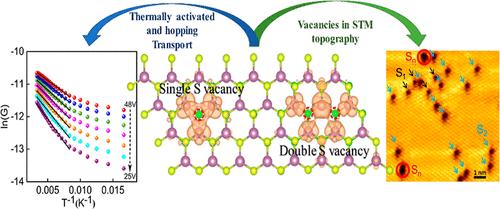
Defects in semiconductors play a crucial role in modifying their electronic structure and transport properties. In transition metal dichalcogenides, atomic chalcogen vacancies are a primary source of intrinsic defects. While the impact of these vacancies on electrical transport has been widely studied, their exact role remains not fully understood. In this work, we correlate optical spectroscopy, low-temperature electrical transport measurements, scanning tunneling microscopy (STM), and first-principles density functional theory (DFT) calculations to explore the effect of chalcogen vacancies in MoS2 monolayers grown by chemical vapor deposition. We specifically highlight the role of disulfur vacancies in modulating electrical properties, showing that these defects increase the density of shallow donor states near the conduction band, which facilitates electron hopping conduction, as evidenced by low-temperature transport and STM measurements. These findings are further supported by DFT calculations, which reveal that the electronic states associated with these defects are relatively delocalized, promoting hopping conduction and inducing n-type doping. This mechanism accounts for the observed high field-effect mobility (>100 cm2 V–1s–1) in the samples. These findings highlight the potential for defect engineering as a universal approach to customizing the properties of 2D materials for various applications.
期刊介绍:
ACS Applied Materials & Interfaces is a leading interdisciplinary journal that brings together chemists, engineers, physicists, and biologists to explore the development and utilization of newly-discovered materials and interfacial processes for specific applications. Our journal has experienced remarkable growth since its establishment in 2009, both in terms of the number of articles published and the impact of the research showcased. We are proud to foster a truly global community, with the majority of published articles originating from outside the United States, reflecting the rapid growth of applied research worldwide.


 分享
分享
 求助内容:
求助内容: 应助结果提醒方式:
 扫码关注我们
