Xuning Zhang, Feixiang Tang, Bo Sun, Xingyue Liu, Guanglan Liao, Weihua Li, Sheng Liu
{"title":"Four-Mask Technique for Manufacturing the Perovskite-on-Silicon Sensor Array for Ultraviolet Light Imaging","authors":"Xuning Zhang, Feixiang Tang, Bo Sun, Xingyue Liu, Guanglan Liao, Weihua Li, Sheng Liu","doi":"10.1002/adfm.202423281","DOIUrl":null,"url":null,"abstract":"<p>Perovskite-based image sensors are widely explored and recognized as the technology of choice for future optoelectronics. Suffering from the incompatibility between perovskite and conventional lithography technology, the challenges of developing high-resolution image sensors come from how to pattern the perovskite film with high precision and integrate it with pixel circuits. Recently, a four-mask technique for manufacturing perovskite-on-silicon sensor arrays, which are composed of a pixeled perovskite film and a planar crossbar circuit is demonstrated. Patterning precision for perovskite films attained 2 µm, ranking top among the previous research. The circuit is also proven to have the highest level of integration, theoretically. A proof-of-concept image sensor showing the first demonstration of monolithic integration of patterned perovskite film with the bottom pixel circuit is successfully made public. Electro-optical performance of its pixels is further characterized and showed high uniformity, benefitting the image sensor in capturing the input light distribution with good spatial resolution. This work has thus set a milestone for perovskite-based image sensors and showed the potential of perovskites in micro-nanoelectronics.</p>","PeriodicalId":112,"journal":{"name":"Advanced Functional Materials","volume":"35 25","pages":""},"PeriodicalIF":19.0000,"publicationDate":"2025-02-17","publicationTypes":"Journal Article","fieldsOfStudy":null,"isOpenAccess":false,"openAccessPdf":"","citationCount":"0","resultStr":null,"platform":"Semanticscholar","paperid":null,"PeriodicalName":"Advanced Functional Materials","FirstCategoryId":"88","ListUrlMain":"https://advanced.onlinelibrary.wiley.com/doi/10.1002/adfm.202423281","RegionNum":1,"RegionCategory":"材料科学","ArticlePicture":[],"TitleCN":null,"AbstractTextCN":null,"PMCID":null,"EPubDate":"","PubModel":"","JCR":"Q1","JCRName":"CHEMISTRY, MULTIDISCIPLINARY","Score":null,"Total":0}
引用次数: 0
Abstract
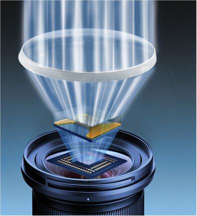
Perovskite-based image sensors are widely explored and recognized as the technology of choice for future optoelectronics. Suffering from the incompatibility between perovskite and conventional lithography technology, the challenges of developing high-resolution image sensors come from how to pattern the perovskite film with high precision and integrate it with pixel circuits. Recently, a four-mask technique for manufacturing perovskite-on-silicon sensor arrays, which are composed of a pixeled perovskite film and a planar crossbar circuit is demonstrated. Patterning precision for perovskite films attained 2 µm, ranking top among the previous research. The circuit is also proven to have the highest level of integration, theoretically. A proof-of-concept image sensor showing the first demonstration of monolithic integration of patterned perovskite film with the bottom pixel circuit is successfully made public. Electro-optical performance of its pixels is further characterized and showed high uniformity, benefitting the image sensor in capturing the input light distribution with good spatial resolution. This work has thus set a milestone for perovskite-based image sensors and showed the potential of perovskites in micro-nanoelectronics.
期刊介绍:
Firmly established as a top-tier materials science journal, Advanced Functional Materials reports breakthrough research in all aspects of materials science, including nanotechnology, chemistry, physics, and biology every week.
Advanced Functional Materials is known for its rapid and fair peer review, quality content, and high impact, making it the first choice of the international materials science community.


 分享
分享
 求助内容:
求助内容: 应助结果提醒方式:
 扫码关注我们
