Hui Shi, Mingyuan Wang, Hongying Chen, Adrien Rousseau, Junpeng Shu, Ming Tian, Ruowang Chen, Juliette Plo, Pierre Valvin, Bernard Gil, Jiajie Qi, Qinghe Wang, Kaihui Liu, Mingliang Zhang, Guillaume Cassabois, Di Wu, Neng Wan
{"title":"Layer-by-Layer Connection for Large Area Single Crystal Boron Nitride Multilayer Films","authors":"Hui Shi, Mingyuan Wang, Hongying Chen, Adrien Rousseau, Junpeng Shu, Ming Tian, Ruowang Chen, Juliette Plo, Pierre Valvin, Bernard Gil, Jiajie Qi, Qinghe Wang, Kaihui Liu, Mingliang Zhang, Guillaume Cassabois, Di Wu, Neng Wan","doi":"10.1021/acsami.4c19877","DOIUrl":null,"url":null,"abstract":"Boron nitride (BN) is today considered one of the most promising materials for many novel applications including bright single photon emission, deep UV optoelectronics, small-sized solid-state neutron detectors, high-performance two-dimensional materials, etc. Recently, AA′ stacking a few layers (2–5 layers) of BN films and ABC stacking multilayer (2.2–12 nm) BN films have been successfully synthesized, respectively. However, the preparation of single crystal metal foil and the subsequent growth of BN thin films are undoubtedly incompatible with the current semiconductor process. In addition, how to achieve an accurate layer-by-layer connection between adjacent multilayer BN domains still needs further research. In this work, we demonstrate an approach to grow large-area multilayer single-crystal BN films by chemical vapor deposition on face-centered cubic Fe–Ni (111) single-crystal alloy thin films with different stoichiometric phases, which are deposited on Sapphire. We show that the BN growth is greatly tunable and improved by increasing the Fe content in single-crystal Fe–Ni (111). The formation of pyramid-shaped multilayer BN domains with aligned orientation enables a continuous connection following a layer-by-layer, “first-meet-first-connect”, mosaic stitching mechanism. By means of selected area electron diffraction, microphotoluminescence spectroscopy in the deep UV, and high-resolution transmission electron microscopy, the layer-by-layer connection mechanism is unambiguously evidenced, and the stacking order has been verified to occur as unidirectional AB and ABC stackings, i.e., in the Bernal and rhombohedral BN phase.","PeriodicalId":5,"journal":{"name":"ACS Applied Materials & Interfaces","volume":"181 1","pages":""},"PeriodicalIF":8.2000,"publicationDate":"2025-02-21","publicationTypes":"Journal Article","fieldsOfStudy":null,"isOpenAccess":false,"openAccessPdf":"","citationCount":"0","resultStr":null,"platform":"Semanticscholar","paperid":null,"PeriodicalName":"ACS Applied Materials & Interfaces","FirstCategoryId":"88","ListUrlMain":"https://doi.org/10.1021/acsami.4c19877","RegionNum":2,"RegionCategory":"材料科学","ArticlePicture":[],"TitleCN":null,"AbstractTextCN":null,"PMCID":null,"EPubDate":"","PubModel":"","JCR":"Q1","JCRName":"MATERIALS SCIENCE, MULTIDISCIPLINARY","Score":null,"Total":0}
引用次数: 0
Abstract
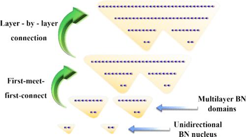
Boron nitride (BN) is today considered one of the most promising materials for many novel applications including bright single photon emission, deep UV optoelectronics, small-sized solid-state neutron detectors, high-performance two-dimensional materials, etc. Recently, AA′ stacking a few layers (2–5 layers) of BN films and ABC stacking multilayer (2.2–12 nm) BN films have been successfully synthesized, respectively. However, the preparation of single crystal metal foil and the subsequent growth of BN thin films are undoubtedly incompatible with the current semiconductor process. In addition, how to achieve an accurate layer-by-layer connection between adjacent multilayer BN domains still needs further research. In this work, we demonstrate an approach to grow large-area multilayer single-crystal BN films by chemical vapor deposition on face-centered cubic Fe–Ni (111) single-crystal alloy thin films with different stoichiometric phases, which are deposited on Sapphire. We show that the BN growth is greatly tunable and improved by increasing the Fe content in single-crystal Fe–Ni (111). The formation of pyramid-shaped multilayer BN domains with aligned orientation enables a continuous connection following a layer-by-layer, “first-meet-first-connect”, mosaic stitching mechanism. By means of selected area electron diffraction, microphotoluminescence spectroscopy in the deep UV, and high-resolution transmission electron microscopy, the layer-by-layer connection mechanism is unambiguously evidenced, and the stacking order has been verified to occur as unidirectional AB and ABC stackings, i.e., in the Bernal and rhombohedral BN phase.
期刊介绍:
ACS Applied Materials & Interfaces is a leading interdisciplinary journal that brings together chemists, engineers, physicists, and biologists to explore the development and utilization of newly-discovered materials and interfacial processes for specific applications. Our journal has experienced remarkable growth since its establishment in 2009, both in terms of the number of articles published and the impact of the research showcased. We are proud to foster a truly global community, with the majority of published articles originating from outside the United States, reflecting the rapid growth of applied research worldwide.


 分享
分享
 求助内容:
求助内容: 应助结果提醒方式:
 扫码关注我们
