Manish Mukherjee, Akshaya Chemmangat, Prashant V. Kamat
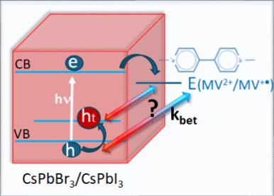
{"title":"Hole Trapping in Lead Halide Perovskite Nanocrystal–Viologen Hybrids and Its Impact on Back Electron Transfer","authors":"Manish Mukherjee, Akshaya Chemmangat, Prashant V. Kamat","doi":"10.1021/acsnano.5c01423","DOIUrl":null,"url":null,"abstract":"Control of forward and back electron transfer processes in semiconductor nanocrystals is important to maximize charge separation for photocatalytic reduction/oxidation processes. By employing methyl viologen as the electron acceptor, we have succeeded in mapping the electron transfer from excited CsPbI<sub>3</sub> nanocrystals to viologen as well as the hole trapping process. The electron transfer to viologen is an ultrafast process (<i>k</i><sub>et</sub> = 2 × 10<sup>10</sup> s<sup>–1</sup>) and results in the formation of extended charge separation as electrons are trapped at surface-bound viologen sites and holes at iodide sites. The I<sub>2</sub><sup>─•</sup> formation, which is confirmed through the transient absorption at 750 nm, provides a convenient way to probe trapped holes and its participation in the back electron transfer process. By employing a series of mixed halide compositions, we were able to tune the bandgap and valence band energy of the perovskite donor. The back electron transfer rate constant (<i>k</i><sub>bet</sub> = 1.3–2.6 × 10<sup>7</sup> s<sup>–1</sup>) is nearly three orders of magnitude smaller than that of forward electron transfer, thus extending the lifetime of the charge-separated state. The weak dependence of the back electron transfer rate constant on the valence band energy suggests that trapping of holes at halide (I or Br) sites is involved in the back electron transfer process. The ability to extend the lifetime of the charge-separated pair can offer new strategies to improve the redox properties of semiconductor-based photocatalytic systems.","PeriodicalId":21,"journal":{"name":"ACS Nano","volume":"2 1","pages":""},"PeriodicalIF":16.0000,"publicationDate":"2025-03-04","publicationTypes":"Journal Article","fieldsOfStudy":null,"isOpenAccess":false,"openAccessPdf":"","citationCount":"0","resultStr":null,"platform":"Semanticscholar","paperid":null,"PeriodicalName":"ACS Nano","FirstCategoryId":"88","ListUrlMain":"https://doi.org/10.1021/acsnano.5c01423","RegionNum":1,"RegionCategory":"材料科学","ArticlePicture":[],"TitleCN":null,"AbstractTextCN":null,"PMCID":null,"EPubDate":"","PubModel":"","JCR":"Q1","JCRName":"CHEMISTRY, MULTIDISCIPLINARY","Score":null,"Total":0}
引用次数: 0
Abstract
Control of forward and back electron transfer processes in semiconductor nanocrystals is important to maximize charge separation for photocatalytic reduction/oxidation processes. By employing methyl viologen as the electron acceptor, we have succeeded in mapping the electron transfer from excited CsPbI3 nanocrystals to viologen as well as the hole trapping process. The electron transfer to viologen is an ultrafast process (ket = 2 × 10¹⁰ s–1) and results in the formation of extended charge separation as electrons are trapped at surface-bound viologen sites and holes at iodide sites. The I2─• formation, which is confirmed through the transient absorption at 750 nm, provides a convenient way to probe trapped holes and its participation in the back electron transfer process. By employing a series of mixed halide compositions, we were able to tune the bandgap and valence band energy of the perovskite donor. The back electron transfer rate constant (kbet = 1.3–2.6 × 10⁷ s–1) is nearly three orders of magnitude smaller than that of forward electron transfer, thus extending the lifetime of the charge-separated state. The weak dependence of the back electron transfer rate constant on the valence band energy suggests that trapping of holes at halide (I or Br) sites is involved in the back electron transfer process. The ability to extend the lifetime of the charge-separated pair can offer new strategies to improve the redox properties of semiconductor-based photocatalytic systems.
期刊介绍:
ACS Nano, published monthly, serves as an international forum for comprehensive articles on nanoscience and nanotechnology research at the intersections of chemistry, biology, materials science, physics, and engineering. The journal fosters communication among scientists in these communities, facilitating collaboration, new research opportunities, and advancements through discoveries. ACS Nano covers synthesis, assembly, characterization, theory, and simulation of nanostructures, nanobiotechnology, nanofabrication, methods and tools for nanoscience and nanotechnology, and self- and directed-assembly. Alongside original research articles, it offers thorough reviews, perspectives on cutting-edge research, and discussions envisioning the future of nanoscience and nanotechnology.


 分享
分享
 求助内容:
求助内容: 应助结果提醒方式:
 扫码关注我们
