{"title":"Zero-dimensionality of a scaled-down VO2 metal-insulator transition via high-resolution electrostatic gating","authors":"Takeaki Yajima, Yusuke Samata, Satoshi Hamasuna, Satya Prakash Pati, Akira Toriumi","doi":"10.1038/s41427-023-00486-9","DOIUrl":null,"url":null,"abstract":"An understanding of the phase transitions at the nanoscale is essential in state-of-the-art engineering1–5, instead of simply averaging the heterogeneous domains formed during phase transitions6,7. However, as materials are scaled down, the steepness of the phase transition rapidly increases8–13 and requires extremely high precision in the control method. Here, a three-terminal device, which could precisely control the phase transition electrically14–19, was applied for the first time to a scaled-down metal-insulator transition material VO2. The crossover from continuous to binary transitions with the scaled-down material was clarified, and the critical channel length was successfully elucidated via phase boundary energy. Notably, below the critical channel length, the spatial degrees of freedom degenerated, and the impact of drain voltage application disappeared in the phase transition, indicating zero-dimensionality of the VO2 channel. This zero-dimensionality could be the fundamental property in the scaled-down phase transition and have a significant impact on various fields that need nanoscale engineering. Controlling the atomic configuration of nanoscale devices to alter their electrical properties has been demonstrated by scientists in Japan. The crystalline structure of a solid can switch between atomic arrangements, or phases, with a change in temperature or electric field. Devices that control these phase transitions have potential applications as computer memories or sensors but such control becomes more difficult as the device gets smaller. Takeaki Yajima from Kyusyu University, Fukuoka, and colleagues have demonstrated the electrically induced change from a metallic to an insulating phase in long, thin, submicrometer vanadium dioxide devices. The team showed that while longer devices exhibited a continuous transition between the two phases as a voltage was applied, the submicrometer devices unexpectedly showed a completely binary switching behavior. Knowing about this different behavior will aid the engineering of nanoscale electronic devices. Although the electrostatic tuning by three-terminal devices is generally weak for phase transition materials, it can control phases with much hither precision than temperature or pressure. This technique was applied to the scaled-down VO2 metal-insulator transitions, where the material phase is controlled by the gate voltage. The crossover from continuous to binary transition with scaling down was demonstrated, and the critical channel length was given by domain boundary instability. Interestingly, below the critical channel length, the influence of the noncritical stimulus (drain voltage in this case) disappeared because the spatial degree of freedom is lost in the single-domain VO2 channel.","PeriodicalId":19382,"journal":{"name":"Npg Asia Materials","volume":"15 1","pages":"1-6"},"PeriodicalIF":8.3000,"publicationDate":"2023-06-30","publicationTypes":"Journal Article","fieldsOfStudy":null,"isOpenAccess":false,"openAccessPdf":"https://www.nature.com/articles/s41427-023-00486-9.pdf","citationCount":"0","resultStr":null,"platform":"Semanticscholar","paperid":null,"PeriodicalName":"Npg Asia Materials","FirstCategoryId":"88","ListUrlMain":"https://www.nature.com/articles/s41427-023-00486-9","RegionNum":2,"RegionCategory":"材料科学","ArticlePicture":[],"TitleCN":null,"AbstractTextCN":null,"PMCID":null,"EPubDate":"","PubModel":"","JCR":"Q1","JCRName":"MATERIALS SCIENCE, MULTIDISCIPLINARY","Score":null,"Total":0}
引用次数: 0
Abstract
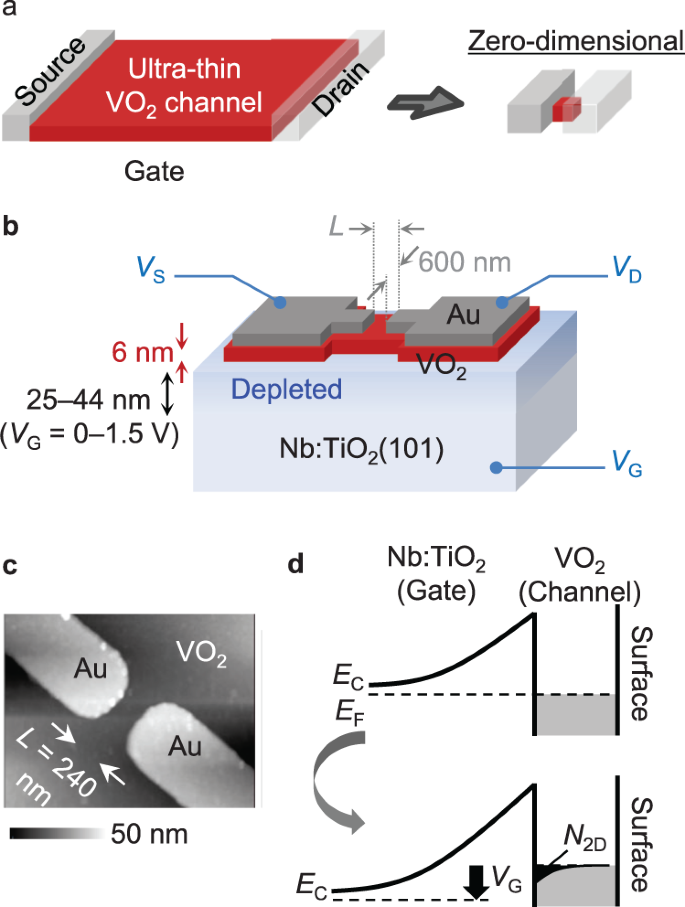
An understanding of the phase transitions at the nanoscale is essential in state-of-the-art engineering1–5, instead of simply averaging the heterogeneous domains formed during phase transitions6,7. However, as materials are scaled down, the steepness of the phase transition rapidly increases8–13 and requires extremely high precision in the control method. Here, a three-terminal device, which could precisely control the phase transition electrically14–19, was applied for the first time to a scaled-down metal-insulator transition material VO2. The crossover from continuous to binary transitions with the scaled-down material was clarified, and the critical channel length was successfully elucidated via phase boundary energy. Notably, below the critical channel length, the spatial degrees of freedom degenerated, and the impact of drain voltage application disappeared in the phase transition, indicating zero-dimensionality of the VO2 channel. This zero-dimensionality could be the fundamental property in the scaled-down phase transition and have a significant impact on various fields that need nanoscale engineering. Controlling the atomic configuration of nanoscale devices to alter their electrical properties has been demonstrated by scientists in Japan. The crystalline structure of a solid can switch between atomic arrangements, or phases, with a change in temperature or electric field. Devices that control these phase transitions have potential applications as computer memories or sensors but such control becomes more difficult as the device gets smaller. Takeaki Yajima from Kyusyu University, Fukuoka, and colleagues have demonstrated the electrically induced change from a metallic to an insulating phase in long, thin, submicrometer vanadium dioxide devices. The team showed that while longer devices exhibited a continuous transition between the two phases as a voltage was applied, the submicrometer devices unexpectedly showed a completely binary switching behavior. Knowing about this different behavior will aid the engineering of nanoscale electronic devices. Although the electrostatic tuning by three-terminal devices is generally weak for phase transition materials, it can control phases with much hither precision than temperature or pressure. This technique was applied to the scaled-down VO2 metal-insulator transitions, where the material phase is controlled by the gate voltage. The crossover from continuous to binary transition with scaling down was demonstrated, and the critical channel length was given by domain boundary instability. Interestingly, below the critical channel length, the influence of the noncritical stimulus (drain voltage in this case) disappeared because the spatial degree of freedom is lost in the single-domain VO2 channel.
期刊介绍:
NPG Asia Materials is an open access, international journal that publishes peer-reviewed review and primary research articles in the field of materials sciences. The journal has a global outlook and reach, with a base in the Asia-Pacific region to reflect the significant and growing output of materials research from this area. The target audience for NPG Asia Materials is scientists and researchers involved in materials research, covering a wide range of disciplines including physical and chemical sciences, biotechnology, and nanotechnology. The journal particularly welcomes high-quality articles from rapidly advancing areas that bridge the gap between materials science and engineering, as well as the classical disciplines of physics, chemistry, and biology. NPG Asia Materials is abstracted/indexed in Journal Citation Reports/Science Edition Web of Knowledge, Google Scholar, Chemical Abstract Services, Scopus, Ulrichsweb (ProQuest), and Scirus.


 分享
分享
 求助内容:
求助内容: 应助结果提醒方式:
 扫码关注我们
