Abdul Ghaffar*, Nihar Ranjan Mohapatra, Ryo Maezono and Kenta Hongo*,
{"title":"WS2 金属触点中费米级析出和界面质量增强的置换掺杂策略","authors":"Abdul Ghaffar*, Nihar Ranjan Mohapatra, Ryo Maezono and Kenta Hongo*, ","doi":"10.1021/acsaelm.4c00609","DOIUrl":null,"url":null,"abstract":"<p >Addressing contact resistance challenges at the interface between metals and transition-metal dichalcogenides (TMDs) remains a complex task due to the persistent Fermi level pinning (FLP) effect near the conduction band minima. Various methods have been explored to mitigate FLP by reducing the chemical interaction between metals and semiconductors. However, these approaches often lead to undesirable consequences, such as reduced adhesion and increased tunneling resistance, ultimately resulting in poor interface quality. A promising solution to overcome these limitations lies in the use of substitutionally doped semiconductor/metal interfaces. We conducted a thorough investigation using first-principles calculations, focusing on S-substituted WS<sub>2</sub>-metal interfaces involving commonly used metals such as Ag, Au, Cu, Pd, Pt, Sc, and Ti. Additionally, we explored the incorporation of nonmetallic dopants, including C, Cl, N, F, O, and P, into the WS<sub>2</sub> surface. Our analysis revolved around several critical parameters, including adhesion strength, Schottky barrier height (SBH), tunnel barrier, charge transfer across the interface, and interface dipole formation. Our study demonstrated that substitutionally doped interfaces can undergo Fermi level depinning while maintaining an enhanced adhesion strength and lower tunneling barrier at the interface. This finding marks a departure from existing methods and offers a promising avenue for inducing p-type contact polarity and addressing contact resistance challenges in TMDs.</p>","PeriodicalId":3,"journal":{"name":"ACS Applied Electronic Materials","volume":"6 6","pages":"4587–4600"},"PeriodicalIF":4.7000,"publicationDate":"2024-05-31","publicationTypes":"Journal Article","fieldsOfStudy":null,"isOpenAccess":false,"openAccessPdf":"https://pubs.acs.org/doi/epdf/10.1021/acsaelm.4c00609","citationCount":"0","resultStr":"{\"title\":\"Substitutional Doping Strategies for Fermi Level Depinning and Enhanced Interface Quality in WS2-Metal Contacts\",\"authors\":\"Abdul Ghaffar*, Nihar Ranjan Mohapatra, Ryo Maezono and Kenta Hongo*, \",\"doi\":\"10.1021/acsaelm.4c00609\",\"DOIUrl\":null,\"url\":null,\"abstract\":\"<p >Addressing contact resistance challenges at the interface between metals and transition-metal dichalcogenides (TMDs) remains a complex task due to the persistent Fermi level pinning (FLP) effect near the conduction band minima. Various methods have been explored to mitigate FLP by reducing the chemical interaction between metals and semiconductors. However, these approaches often lead to undesirable consequences, such as reduced adhesion and increased tunneling resistance, ultimately resulting in poor interface quality. A promising solution to overcome these limitations lies in the use of substitutionally doped semiconductor/metal interfaces. We conducted a thorough investigation using first-principles calculations, focusing on S-substituted WS<sub>2</sub>-metal interfaces involving commonly used metals such as Ag, Au, Cu, Pd, Pt, Sc, and Ti. Additionally, we explored the incorporation of nonmetallic dopants, including C, Cl, N, F, O, and P, into the WS<sub>2</sub> surface. Our analysis revolved around several critical parameters, including adhesion strength, Schottky barrier height (SBH), tunnel barrier, charge transfer across the interface, and interface dipole formation. Our study demonstrated that substitutionally doped interfaces can undergo Fermi level depinning while maintaining an enhanced adhesion strength and lower tunneling barrier at the interface. This finding marks a departure from existing methods and offers a promising avenue for inducing p-type contact polarity and addressing contact resistance challenges in TMDs.</p>\",\"PeriodicalId\":3,\"journal\":{\"name\":\"ACS Applied Electronic Materials\",\"volume\":\"6 6\",\"pages\":\"4587–4600\"},\"PeriodicalIF\":4.7000,\"publicationDate\":\"2024-05-31\",\"publicationTypes\":\"Journal Article\",\"fieldsOfStudy\":null,\"isOpenAccess\":false,\"openAccessPdf\":\"https://pubs.acs.org/doi/epdf/10.1021/acsaelm.4c00609\",\"citationCount\":\"0\",\"resultStr\":null,\"platform\":\"Semanticscholar\",\"paperid\":null,\"PeriodicalName\":\"ACS Applied Electronic Materials\",\"FirstCategoryId\":\"88\",\"ListUrlMain\":\"https://pubs.acs.org/doi/10.1021/acsaelm.4c00609\",\"RegionNum\":3,\"RegionCategory\":\"材料科学\",\"ArticlePicture\":[],\"TitleCN\":null,\"AbstractTextCN\":null,\"PMCID\":null,\"EPubDate\":\"\",\"PubModel\":\"\",\"JCR\":\"Q1\",\"JCRName\":\"ENGINEERING, ELECTRICAL & ELECTRONIC\",\"Score\":null,\"Total\":0}","platform":"Semanticscholar","paperid":null,"PeriodicalName":"ACS Applied Electronic Materials","FirstCategoryId":"88","ListUrlMain":"https://pubs.acs.org/doi/10.1021/acsaelm.4c00609","RegionNum":3,"RegionCategory":"材料科学","ArticlePicture":[],"TitleCN":null,"AbstractTextCN":null,"PMCID":null,"EPubDate":"","PubModel":"","JCR":"Q1","JCRName":"ENGINEERING, ELECTRICAL & ELECTRONIC","Score":null,"Total":0}
引用次数: 0
摘要
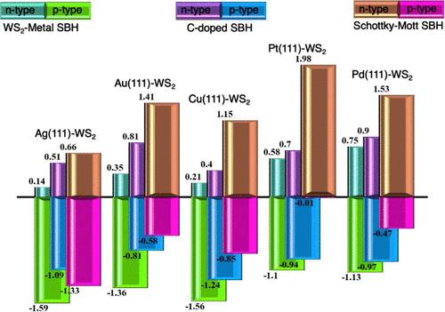
由于在导带极小值附近存在持续的费米级针销(FLP)效应,解决金属与过渡金属二掺杂化合物(TMDs)界面上的接触电阻问题仍然是一项复杂的任务。人们探索了各种方法,通过减少金属与半导体之间的化学作用来减轻费米级钉住效应。然而,这些方法往往会导致不良后果,如附着力降低和隧穿电阻增加,最终导致界面质量低下。要克服这些限制,一种很有前景的解决方案是使用替代掺杂的半导体/金属界面。我们利用第一原理计算进行了深入研究,重点关注 S 取代的 WS2-金属界面,涉及 Ag、Au、Cu、Pd、Pt、Sc 和 Ti 等常用金属。此外,我们还探讨了在 WS2 表面掺入非金属掺杂剂的问题,包括 C、Cl、N、F、O 和 P。我们的分析围绕几个关键参数展开,包括附着强度、肖特基势垒高度(SBH)、隧道势垒、跨界面电荷转移和界面偶极子形成。我们的研究表明,替代掺杂的界面在保持增强的粘附强度和较低的界面隧道势垒的同时,还能发生费米级去稀化。这一发现标志着与现有方法的不同,为在 TMD 中诱导 p 型接触极性和解决接触电阻难题提供了一条前景广阔的途径。
Substitutional Doping Strategies for Fermi Level Depinning and Enhanced Interface Quality in WS2-Metal Contacts
Addressing contact resistance challenges at the interface between metals and transition-metal dichalcogenides (TMDs) remains a complex task due to the persistent Fermi level pinning (FLP) effect near the conduction band minima. Various methods have been explored to mitigate FLP by reducing the chemical interaction between metals and semiconductors. However, these approaches often lead to undesirable consequences, such as reduced adhesion and increased tunneling resistance, ultimately resulting in poor interface quality. A promising solution to overcome these limitations lies in the use of substitutionally doped semiconductor/metal interfaces. We conducted a thorough investigation using first-principles calculations, focusing on S-substituted WS2-metal interfaces involving commonly used metals such as Ag, Au, Cu, Pd, Pt, Sc, and Ti. Additionally, we explored the incorporation of nonmetallic dopants, including C, Cl, N, F, O, and P, into the WS2 surface. Our analysis revolved around several critical parameters, including adhesion strength, Schottky barrier height (SBH), tunnel barrier, charge transfer across the interface, and interface dipole formation. Our study demonstrated that substitutionally doped interfaces can undergo Fermi level depinning while maintaining an enhanced adhesion strength and lower tunneling barrier at the interface. This finding marks a departure from existing methods and offers a promising avenue for inducing p-type contact polarity and addressing contact resistance challenges in TMDs.
期刊介绍:
ACS Applied Electronic Materials is an interdisciplinary journal publishing original research covering all aspects of electronic materials. The journal is devoted to reports of new and original experimental and theoretical research of an applied nature that integrate knowledge in the areas of materials science, engineering, optics, physics, and chemistry into important applications of electronic materials. Sample research topics that span the journal's scope are inorganic, organic, ionic and polymeric materials with properties that include conducting, semiconducting, superconducting, insulating, dielectric, magnetic, optoelectronic, piezoelectric, ferroelectric and thermoelectric.
Indexed/Abstracted:
Web of Science SCIE
Scopus
CAS
INSPEC
Portico


 分享
分享
 求助内容:
求助内容: 应助结果提醒方式:
 扫码关注我们
