Rahmat Hadi Saputro, Tatsuro Maeda, Kaoru Toko, Ryo Matsumura* and Naoki Fukata*,
{"title":"通过高速连续波激光退火实现拉伸应变 n-Ge 合金中的高掺杂活化(≥1020 cm-3","authors":"Rahmat Hadi Saputro, Tatsuro Maeda, Kaoru Toko, Ryo Matsumura* and Naoki Fukata*, ","doi":"10.1021/acsaelm.4c00399","DOIUrl":null,"url":null,"abstract":"<p >Germanium-based materials are essential for the integration of Group IV optoelectronics in silicon devices. In addition to tensile strain, high n-type doping is critical, as it provides abundant carriers for recombination, potentially enabling higher photoemissions from Ge-based materials. We report here record-high 68% doping activation on n-Ge with ≥10<sup>20</sup> cm<sup>–3</sup> carrier density. This study centers on Sb-doped n-type Ge-on-insulator thin films with Si or Sn alloying grown using high-speed continuous-wave laser annealing (CWLA). Crystal mapping revealed the growth of polycrystalline n-GeSn and n-GeSi thin films with grain sizes up to 4 μm in diameter. Micro-PL measurements showed the PL intensity of n-Ge to be enhanced by the alloying of Sn and Si, with peak intensity 1.5 and 3 times higher for n-GeSn and n-GeSi, respectively. Raman peak red shift and broadening are observed in the samples, indicating high tensile strain and n-type doping. The measured carrier density of CWLA-grown films aligns well with the PL intensity trend, suggesting the process has promise for achieving electrically improved Ge-based thin films.</p>","PeriodicalId":3,"journal":{"name":"ACS Applied Electronic Materials","volume":"6 6","pages":"4297–4303"},"PeriodicalIF":4.7000,"publicationDate":"2024-06-03","publicationTypes":"Journal Article","fieldsOfStudy":null,"isOpenAccess":false,"openAccessPdf":"","citationCount":"0","resultStr":"{\"title\":\"High Doping Activation (≥1020 cm–3) in Tensile-Strained n-Ge Alloys Achieved by High-Speed Continuous-Wave Laser Annealing\",\"authors\":\"Rahmat Hadi Saputro, Tatsuro Maeda, Kaoru Toko, Ryo Matsumura* and Naoki Fukata*, \",\"doi\":\"10.1021/acsaelm.4c00399\",\"DOIUrl\":null,\"url\":null,\"abstract\":\"<p >Germanium-based materials are essential for the integration of Group IV optoelectronics in silicon devices. In addition to tensile strain, high n-type doping is critical, as it provides abundant carriers for recombination, potentially enabling higher photoemissions from Ge-based materials. We report here record-high 68% doping activation on n-Ge with ≥10<sup>20</sup> cm<sup>–3</sup> carrier density. This study centers on Sb-doped n-type Ge-on-insulator thin films with Si or Sn alloying grown using high-speed continuous-wave laser annealing (CWLA). Crystal mapping revealed the growth of polycrystalline n-GeSn and n-GeSi thin films with grain sizes up to 4 μm in diameter. Micro-PL measurements showed the PL intensity of n-Ge to be enhanced by the alloying of Sn and Si, with peak intensity 1.5 and 3 times higher for n-GeSn and n-GeSi, respectively. Raman peak red shift and broadening are observed in the samples, indicating high tensile strain and n-type doping. The measured carrier density of CWLA-grown films aligns well with the PL intensity trend, suggesting the process has promise for achieving electrically improved Ge-based thin films.</p>\",\"PeriodicalId\":3,\"journal\":{\"name\":\"ACS Applied Electronic Materials\",\"volume\":\"6 6\",\"pages\":\"4297–4303\"},\"PeriodicalIF\":4.7000,\"publicationDate\":\"2024-06-03\",\"publicationTypes\":\"Journal Article\",\"fieldsOfStudy\":null,\"isOpenAccess\":false,\"openAccessPdf\":\"\",\"citationCount\":\"0\",\"resultStr\":null,\"platform\":\"Semanticscholar\",\"paperid\":null,\"PeriodicalName\":\"ACS Applied Electronic Materials\",\"FirstCategoryId\":\"88\",\"ListUrlMain\":\"https://pubs.acs.org/doi/10.1021/acsaelm.4c00399\",\"RegionNum\":3,\"RegionCategory\":\"材料科学\",\"ArticlePicture\":[],\"TitleCN\":null,\"AbstractTextCN\":null,\"PMCID\":null,\"EPubDate\":\"\",\"PubModel\":\"\",\"JCR\":\"Q1\",\"JCRName\":\"ENGINEERING, ELECTRICAL & ELECTRONIC\",\"Score\":null,\"Total\":0}","platform":"Semanticscholar","paperid":null,"PeriodicalName":"ACS Applied Electronic Materials","FirstCategoryId":"88","ListUrlMain":"https://pubs.acs.org/doi/10.1021/acsaelm.4c00399","RegionNum":3,"RegionCategory":"材料科学","ArticlePicture":[],"TitleCN":null,"AbstractTextCN":null,"PMCID":null,"EPubDate":"","PubModel":"","JCR":"Q1","JCRName":"ENGINEERING, ELECTRICAL & ELECTRONIC","Score":null,"Total":0}
引用次数: 0
摘要
锗基材料对于在硅器件中集成第四族光电子技术至关重要。除了拉伸应变之外,高 n 型掺杂也至关重要,因为它能为重组提供丰富的载流子,从而有可能使锗基材料产生更高的光辐射。我们在此报告了载流子密度≥1020 cm-3 的 n-Ge 上创纪录的 68% 掺杂活化率。这项研究的核心是使用高速连续波激光退火(CWLA)技术生长的掺锑 n 型绝缘体锗薄膜,其中含有硅或锡合金。晶体图显示生长出了晶粒直径达 4 μm 的多晶 n-GeSn 和 n-GeSi 薄膜。显微光致发光测量显示,正锗的光致发光强度因锡和硅的合金化而增强,正锗硒和正锗硅的峰值强度分别高出 1.5 倍和 3 倍。在样品中观察到拉曼峰红移和展宽,表明样品具有较高的拉伸应变和 n 型掺杂。测量到的 CWLA 生长薄膜的载流子密度与 PL 强度趋势非常吻合,这表明该工艺有望实现电性改进的 Ge 基薄膜。
High Doping Activation (≥1020 cm–3) in Tensile-Strained n-Ge Alloys Achieved by High-Speed Continuous-Wave Laser Annealing
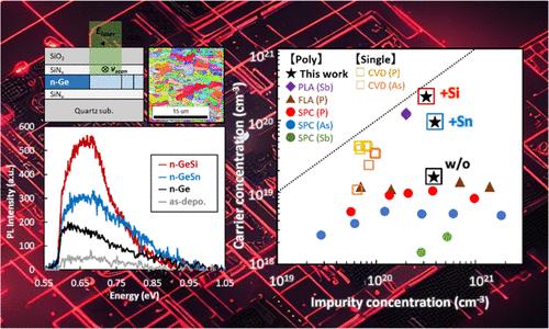
Germanium-based materials are essential for the integration of Group IV optoelectronics in silicon devices. In addition to tensile strain, high n-type doping is critical, as it provides abundant carriers for recombination, potentially enabling higher photoemissions from Ge-based materials. We report here record-high 68% doping activation on n-Ge with ≥1020 cm–3 carrier density. This study centers on Sb-doped n-type Ge-on-insulator thin films with Si or Sn alloying grown using high-speed continuous-wave laser annealing (CWLA). Crystal mapping revealed the growth of polycrystalline n-GeSn and n-GeSi thin films with grain sizes up to 4 μm in diameter. Micro-PL measurements showed the PL intensity of n-Ge to be enhanced by the alloying of Sn and Si, with peak intensity 1.5 and 3 times higher for n-GeSn and n-GeSi, respectively. Raman peak red shift and broadening are observed in the samples, indicating high tensile strain and n-type doping. The measured carrier density of CWLA-grown films aligns well with the PL intensity trend, suggesting the process has promise for achieving electrically improved Ge-based thin films.
期刊介绍:
ACS Applied Electronic Materials is an interdisciplinary journal publishing original research covering all aspects of electronic materials. The journal is devoted to reports of new and original experimental and theoretical research of an applied nature that integrate knowledge in the areas of materials science, engineering, optics, physics, and chemistry into important applications of electronic materials. Sample research topics that span the journal's scope are inorganic, organic, ionic and polymeric materials with properties that include conducting, semiconducting, superconducting, insulating, dielectric, magnetic, optoelectronic, piezoelectric, ferroelectric and thermoelectric.
Indexed/Abstracted:
Web of Science SCIE
Scopus
CAS
INSPEC
Portico


 分享
分享
 求助内容:
求助内容: 应助结果提醒方式:
 扫码关注我们
