Kunyang Li , Shuying Deng , Aiqin Zhang , Jinjiang Fu , Junyao Luo , Xuehao Chen , Jianying Zhou , Zhou Zhou
{"title":"结合维纳解卷积和照明优化进行掩膜缺陷检测","authors":"Kunyang Li , Shuying Deng , Aiqin Zhang , Jinjiang Fu , Junyao Luo , Xuehao Chen , Jianying Zhou , Zhou Zhou","doi":"10.1016/j.mee.2024.112245","DOIUrl":null,"url":null,"abstract":"<div><p>In the lithography process, mask defect is inevitably replicated on chips hence the yield and quality of the product are directly related to the mask quality. Mask microscopy resolution is then an essential specification. In this work, a high-efficiency method for enhancing the resolution of mask defect is proposed based on illumination optimization and Wiener deconvolution. To validate this approach, we established a verification apparatus designed to achieve a theoretical resolution of 3.0 μm with visible light. Remarkably, the empirical results demonstrated that the actual resolution attained is as low as 2.5 μm. The verification demonstrates a significant improvement for various periodic fringes. Moreover, the augmented capability of the apparatus facilitates the identification of mask defects. Although the experiment is carried out for the visible wavelength, the research is specifically designed for the working conditions suitable for EUV mask detection based on the preparatory work for the EUV.</p></div>","PeriodicalId":18557,"journal":{"name":"Microelectronic Engineering","volume":"293 ","pages":"Article 112245"},"PeriodicalIF":3.1000,"publicationDate":"2024-10-01","publicationTypes":"Journal Article","fieldsOfStudy":null,"isOpenAccess":false,"openAccessPdf":"https://www.sciencedirect.com/science/article/pii/S016793172400114X/pdfft?md5=67621d3a1e265d22316b27b27cff04b9&pid=1-s2.0-S016793172400114X-main.pdf","citationCount":"0","resultStr":"{\"title\":\"Mask defect detection by combining wiener deconvolution and illumination optimization\",\"authors\":\"Kunyang Li , Shuying Deng , Aiqin Zhang , Jinjiang Fu , Junyao Luo , Xuehao Chen , Jianying Zhou , Zhou Zhou\",\"doi\":\"10.1016/j.mee.2024.112245\",\"DOIUrl\":null,\"url\":null,\"abstract\":\"<div><p>In the lithography process, mask defect is inevitably replicated on chips hence the yield and quality of the product are directly related to the mask quality. Mask microscopy resolution is then an essential specification. In this work, a high-efficiency method for enhancing the resolution of mask defect is proposed based on illumination optimization and Wiener deconvolution. To validate this approach, we established a verification apparatus designed to achieve a theoretical resolution of 3.0 μm with visible light. Remarkably, the empirical results demonstrated that the actual resolution attained is as low as 2.5 μm. The verification demonstrates a significant improvement for various periodic fringes. Moreover, the augmented capability of the apparatus facilitates the identification of mask defects. Although the experiment is carried out for the visible wavelength, the research is specifically designed for the working conditions suitable for EUV mask detection based on the preparatory work for the EUV.</p></div>\",\"PeriodicalId\":18557,\"journal\":{\"name\":\"Microelectronic Engineering\",\"volume\":\"293 \",\"pages\":\"Article 112245\"},\"PeriodicalIF\":3.1000,\"publicationDate\":\"2024-10-01\",\"publicationTypes\":\"Journal Article\",\"fieldsOfStudy\":null,\"isOpenAccess\":false,\"openAccessPdf\":\"https://www.sciencedirect.com/science/article/pii/S016793172400114X/pdfft?md5=67621d3a1e265d22316b27b27cff04b9&pid=1-s2.0-S016793172400114X-main.pdf\",\"citationCount\":\"0\",\"resultStr\":null,\"platform\":\"Semanticscholar\",\"paperid\":null,\"PeriodicalName\":\"Microelectronic Engineering\",\"FirstCategoryId\":\"5\",\"ListUrlMain\":\"https://www.sciencedirect.com/science/article/pii/S016793172400114X\",\"RegionNum\":4,\"RegionCategory\":\"工程技术\",\"ArticlePicture\":[],\"TitleCN\":null,\"AbstractTextCN\":null,\"PMCID\":null,\"EPubDate\":\"2024/7/15 0:00:00\",\"PubModel\":\"Epub\",\"JCR\":\"Q2\",\"JCRName\":\"ENGINEERING, ELECTRICAL & ELECTRONIC\",\"Score\":null,\"Total\":0}","platform":"Semanticscholar","paperid":null,"PeriodicalName":"Microelectronic Engineering","FirstCategoryId":"5","ListUrlMain":"https://www.sciencedirect.com/science/article/pii/S016793172400114X","RegionNum":4,"RegionCategory":"工程技术","ArticlePicture":[],"TitleCN":null,"AbstractTextCN":null,"PMCID":null,"EPubDate":"2024/7/15 0:00:00","PubModel":"Epub","JCR":"Q2","JCRName":"ENGINEERING, ELECTRICAL & ELECTRONIC","Score":null,"Total":0}
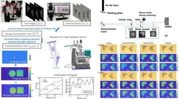
Mask defect detection by combining wiener deconvolution and illumination optimization
In the lithography process, mask defect is inevitably replicated on chips hence the yield and quality of the product are directly related to the mask quality. Mask microscopy resolution is then an essential specification. In this work, a high-efficiency method for enhancing the resolution of mask defect is proposed based on illumination optimization and Wiener deconvolution. To validate this approach, we established a verification apparatus designed to achieve a theoretical resolution of 3.0 μm with visible light. Remarkably, the empirical results demonstrated that the actual resolution attained is as low as 2.5 μm. The verification demonstrates a significant improvement for various periodic fringes. Moreover, the augmented capability of the apparatus facilitates the identification of mask defects. Although the experiment is carried out for the visible wavelength, the research is specifically designed for the working conditions suitable for EUV mask detection based on the preparatory work for the EUV.
期刊介绍:
Microelectronic Engineering is the premier nanoprocessing, and nanotechnology journal focusing on fabrication of electronic, photonic, bioelectronic, electromechanic and fluidic devices and systems, and their applications in the broad areas of electronics, photonics, energy, life sciences, and environment. It covers also the expanding interdisciplinary field of "more than Moore" and "beyond Moore" integrated nanoelectronics / photonics and micro-/nano-/bio-systems. Through its unique mixture of peer-reviewed articles, reviews, accelerated publications, short and Technical notes, and the latest research news on key developments, Microelectronic Engineering provides comprehensive coverage of this exciting, interdisciplinary and dynamic new field for researchers in academia and professionals in industry.


 分享
分享
 求助内容:
求助内容: 应助结果提醒方式:
 扫码关注我们
