{"title":"Numerical investigation of energy level strategy for TMO/Si tunneling heterojunction solar cells","authors":"Zhongliang Gao, GuiJia Feng, Hui Zhou, Li Ding","doi":"10.1007/s10825-024-02128-x","DOIUrl":null,"url":null,"abstract":"<div><p>A thin film of transition metal oxide (TMO) layer forms a heterojunction configuration with silicon (Si) via dopant-free fabrication process. However, excellent hole selective contact performance of TMO/<i>n</i>-Si heterojunction necessitates a stringent alignment of energy levels. Herein, we studied the level matching strategy of TMO/<i>n</i>-Si heterojunction with four parameters including conduction band (<i>E</i><sub>C</sub>), bandgap (<i>E</i><sub><i>g</i></sub>), Fermi level (<i>E</i><sub>F</sub>) and interface trap concentration (<i>N</i><sub>t</sub>). It is found that the electron affinity (<i>E</i><sub>a</sub>) of TMO determines the relative position of the energy level, and increasing the <i>E</i><sub>a</sub> can increase the open-circuit voltage (<i>V</i><sub>OC</sub>) from 426.0 to 742.5 mV. In addition, the energy level bending of the interface can be adjusted by the relative <i>E</i><sub>F</sub> position of TMO and <i>n</i>-Si to improve the carrier separation efficiency to increase the short-circuit current density (<i>J</i><sub>SC</sub>). Meanwhile, the higher <i>N</i><sub>t</sub> is beneficial to the carrier tunneling transport in the case of <i>E</i><sub>C</sub> of TMO being smaller than that of <i>n</i>-Si, which enhances the energy level bending of the interface and improves the solar cells performance. Finally, the MoO<sub><i>x</i></sub>/<i>n</i>-Si heterojunction solar cell is optimized to obtained the power conversion efficiency (PCE) of 21.87%.</p></div>","PeriodicalId":620,"journal":{"name":"Journal of Computational Electronics","volume":"23 2","pages":"369 - 381"},"PeriodicalIF":2.5000,"publicationDate":"2024-02-02","publicationTypes":"Journal Article","fieldsOfStudy":null,"isOpenAccess":false,"openAccessPdf":"","citationCount":"0","resultStr":null,"platform":"Semanticscholar","paperid":null,"PeriodicalName":"Journal of Computational Electronics","FirstCategoryId":"5","ListUrlMain":"https://link.springer.com/article/10.1007/s10825-024-02128-x","RegionNum":4,"RegionCategory":"工程技术","ArticlePicture":[],"TitleCN":null,"AbstractTextCN":null,"PMCID":null,"EPubDate":"","PubModel":"","JCR":"Q3","JCRName":"ENGINEERING, ELECTRICAL & ELECTRONIC","Score":null,"Total":0}
引用次数: 0
Abstract
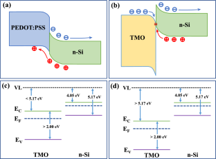
A thin film of transition metal oxide (TMO) layer forms a heterojunction configuration with silicon (Si) via dopant-free fabrication process. However, excellent hole selective contact performance of TMO/n-Si heterojunction necessitates a stringent alignment of energy levels. Herein, we studied the level matching strategy of TMO/n-Si heterojunction with four parameters including conduction band (EC), bandgap (Eg), Fermi level (EF) and interface trap concentration (Nt). It is found that the electron affinity (Ea) of TMO determines the relative position of the energy level, and increasing the Ea can increase the open-circuit voltage (VOC) from 426.0 to 742.5 mV. In addition, the energy level bending of the interface can be adjusted by the relative EF position of TMO and n-Si to improve the carrier separation efficiency to increase the short-circuit current density (JSC). Meanwhile, the higher Nt is beneficial to the carrier tunneling transport in the case of EC of TMO being smaller than that of n-Si, which enhances the energy level bending of the interface and improves the solar cells performance. Finally, the MoOx/n-Si heterojunction solar cell is optimized to obtained the power conversion efficiency (PCE) of 21.87%.
期刊介绍:
he Journal of Computational Electronics brings together research on all aspects of modeling and simulation of modern electronics. This includes optical, electronic, mechanical, and quantum mechanical aspects, as well as research on the underlying mathematical algorithms and computational details. The related areas of energy conversion/storage and of molecular and biological systems, in which the thrust is on the charge transport, electronic, mechanical, and optical properties, are also covered.
In particular, we encourage manuscripts dealing with device simulation; with optical and optoelectronic systems and photonics; with energy storage (e.g. batteries, fuel cells) and harvesting (e.g. photovoltaic), with simulation of circuits, VLSI layout, logic and architecture (based on, for example, CMOS devices, quantum-cellular automata, QBITs, or single-electron transistors); with electromagnetic simulations (such as microwave electronics and components); or with molecular and biological systems. However, in all these cases, the submitted manuscripts should explicitly address the electronic properties of the relevant systems, materials, or devices and/or present novel contributions to the physical models, computational strategies, or numerical algorithms.


 分享
分享
 求助内容:
求助内容: 应助结果提醒方式:
 扫码关注我们
