{"title":"Nanoimprint-induced strain engineering of two-dimensional materials","authors":"Chuying Sun, Jianwen Zhong, Zhuofei Gan, Liyang Chen, Chuwei Liang, Hongtao Feng, Zhao Sun, Zijie Jiang, Wen-Di Li","doi":"10.1038/s41378-024-00669-6","DOIUrl":null,"url":null,"abstract":"<p>The high stretchability of two-dimensional (2D) materials has facilitated the possibility of using external strain to manipulate their properties. Hence, strain engineering has emerged as a promising technique for tailoring the performance of 2D materials by controlling the applied elastic strain field. Although various types of strain engineering methods have been proposed, deterministic and controllable generation of the strain in 2D materials remains a challenging task. Here, we report a nanoimprint-induced strain engineering (NISE) strategy for introducing controllable periodic strain profiles on 2D materials. A three-dimensional (3D) tunable strain is generated in a molybdenum disulfide (MoS<sub>2</sub>) sheet by pressing and conforming to the topography of an imprint mold. Different strain profiles generated in MoS<sub>2</sub> are demonstrated and verified by Raman and photoluminescence (PL) spectroscopy. The strain modulation capability of NISE is investigated by changing the imprint pressure and the patterns of the imprint molds, which enables precise control of the strain magnitudes and distributions in MoS<sub>2</sub>. Furthermore, a finite element model is developed to simulate the NISE process and reveal the straining behavior of MoS<sub>2</sub>. This deterministic and effective strain engineering technique can be easily extended to other materials and is also compatible with common semiconductor fabrication processes; therefore, it provides prospects for advances in broad nanoelectronic and optoelectronic devices.</p><figure></figure>","PeriodicalId":18560,"journal":{"name":"Microsystems & Nanoengineering","volume":"47 1","pages":""},"PeriodicalIF":9.9000,"publicationDate":"2024-04-08","publicationTypes":"Journal Article","fieldsOfStudy":null,"isOpenAccess":false,"openAccessPdf":"","citationCount":"0","resultStr":null,"platform":"Semanticscholar","paperid":null,"PeriodicalName":"Microsystems & Nanoengineering","FirstCategoryId":"5","ListUrlMain":"https://doi.org/10.1038/s41378-024-00669-6","RegionNum":1,"RegionCategory":"工程技术","ArticlePicture":[],"TitleCN":null,"AbstractTextCN":null,"PMCID":null,"EPubDate":"","PubModel":"","JCR":"Q1","JCRName":"INSTRUMENTS & INSTRUMENTATION","Score":null,"Total":0}
引用次数: 0
Abstract
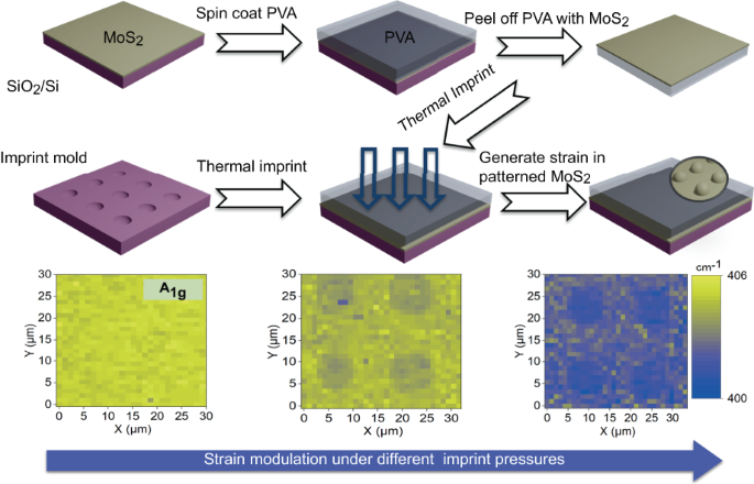
The high stretchability of two-dimensional (2D) materials has facilitated the possibility of using external strain to manipulate their properties. Hence, strain engineering has emerged as a promising technique for tailoring the performance of 2D materials by controlling the applied elastic strain field. Although various types of strain engineering methods have been proposed, deterministic and controllable generation of the strain in 2D materials remains a challenging task. Here, we report a nanoimprint-induced strain engineering (NISE) strategy for introducing controllable periodic strain profiles on 2D materials. A three-dimensional (3D) tunable strain is generated in a molybdenum disulfide (MoS2) sheet by pressing and conforming to the topography of an imprint mold. Different strain profiles generated in MoS2 are demonstrated and verified by Raman and photoluminescence (PL) spectroscopy. The strain modulation capability of NISE is investigated by changing the imprint pressure and the patterns of the imprint molds, which enables precise control of the strain magnitudes and distributions in MoS2. Furthermore, a finite element model is developed to simulate the NISE process and reveal the straining behavior of MoS2. This deterministic and effective strain engineering technique can be easily extended to other materials and is also compatible with common semiconductor fabrication processes; therefore, it provides prospects for advances in broad nanoelectronic and optoelectronic devices.
期刊介绍:
Microsystems & Nanoengineering is a comprehensive online journal that focuses on the field of Micro and Nano Electro Mechanical Systems (MEMS and NEMS). It provides a platform for researchers to share their original research findings and review articles in this area. The journal covers a wide range of topics, from fundamental research to practical applications. Published by Springer Nature, in collaboration with the Aerospace Information Research Institute, Chinese Academy of Sciences, and with the support of the State Key Laboratory of Transducer Technology, it is an esteemed publication in the field. As an open access journal, it offers free access to its content, allowing readers from around the world to benefit from the latest developments in MEMS and NEMS.


 分享
分享
 求助内容:
求助内容: 应助结果提醒方式:
 扫码关注我们
