Chenxu Zhu, Huseyin Ekinci, Aixi Pan, Bo Cui, Xiaoli Zhu
{"title":"Electron beam lithography on nonplanar and irregular surfaces","authors":"Chenxu Zhu, Huseyin Ekinci, Aixi Pan, Bo Cui, Xiaoli Zhu","doi":"10.1038/s41378-024-00682-9","DOIUrl":null,"url":null,"abstract":"<p>E-beam lithography is a powerful tool for generating nanostructures and fabricating nanodevices with fine features approaching a few nanometers in size. However, alternative approaches to conventional spin coating and development processes are required to optimize the lithography procedure on irregular surfaces. In this review, we summarize the state of the art in nanofabrication on irregular substrates using e-beam lithography. To overcome these challenges, unconventional methods have been developed. For instance, polymeric and nonpolymeric materials can be sprayed or evaporated to form uniform layers of electron-sensitive materials on irregular substrates. Moreover, chemical bonds can be applied to help form polymer brushes or self-assembled monolayers on these surfaces. In addition, thermal oxides can serve as resists, as the etching rate in solution changes after e-beam exposure. Furthermore, e-beam lithography tools can be combined with cryostages, evaporation systems, and metal deposition chambers for sample development and lift-off while maintaining low temperatures. Metallic nanopyramids can be fabricated on an AFM tip by utilizing ice as a positive resistor. Additionally, Ti/Au caps can be patterned around a carbon nanotube. Moreover, 3D nanostructures can be formed on irregular surfaces by exposing layers of anisole on organic ice surfaces with a focused e-beam. These advances in e-beam lithography on irregular substrates, including uniform film coating, instrumentation improvement, and new pattern transferring method development, substantially extend its capabilities in the fabrication and application of nanoscale structures.</p><figure></figure>","PeriodicalId":18560,"journal":{"name":"Microsystems & Nanoengineering","volume":"100 1","pages":""},"PeriodicalIF":9.9000,"publicationDate":"2024-04-19","publicationTypes":"Journal Article","fieldsOfStudy":null,"isOpenAccess":false,"openAccessPdf":"","citationCount":"0","resultStr":null,"platform":"Semanticscholar","paperid":null,"PeriodicalName":"Microsystems & Nanoengineering","FirstCategoryId":"5","ListUrlMain":"https://doi.org/10.1038/s41378-024-00682-9","RegionNum":1,"RegionCategory":"工程技术","ArticlePicture":[],"TitleCN":null,"AbstractTextCN":null,"PMCID":null,"EPubDate":"","PubModel":"","JCR":"Q1","JCRName":"INSTRUMENTS & INSTRUMENTATION","Score":null,"Total":0}
引用次数: 0
Abstract
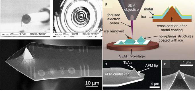
E-beam lithography is a powerful tool for generating nanostructures and fabricating nanodevices with fine features approaching a few nanometers in size. However, alternative approaches to conventional spin coating and development processes are required to optimize the lithography procedure on irregular surfaces. In this review, we summarize the state of the art in nanofabrication on irregular substrates using e-beam lithography. To overcome these challenges, unconventional methods have been developed. For instance, polymeric and nonpolymeric materials can be sprayed or evaporated to form uniform layers of electron-sensitive materials on irregular substrates. Moreover, chemical bonds can be applied to help form polymer brushes or self-assembled monolayers on these surfaces. In addition, thermal oxides can serve as resists, as the etching rate in solution changes after e-beam exposure. Furthermore, e-beam lithography tools can be combined with cryostages, evaporation systems, and metal deposition chambers for sample development and lift-off while maintaining low temperatures. Metallic nanopyramids can be fabricated on an AFM tip by utilizing ice as a positive resistor. Additionally, Ti/Au caps can be patterned around a carbon nanotube. Moreover, 3D nanostructures can be formed on irregular surfaces by exposing layers of anisole on organic ice surfaces with a focused e-beam. These advances in e-beam lithography on irregular substrates, including uniform film coating, instrumentation improvement, and new pattern transferring method development, substantially extend its capabilities in the fabrication and application of nanoscale structures.
期刊介绍:
Microsystems & Nanoengineering is a comprehensive online journal that focuses on the field of Micro and Nano Electro Mechanical Systems (MEMS and NEMS). It provides a platform for researchers to share their original research findings and review articles in this area. The journal covers a wide range of topics, from fundamental research to practical applications. Published by Springer Nature, in collaboration with the Aerospace Information Research Institute, Chinese Academy of Sciences, and with the support of the State Key Laboratory of Transducer Technology, it is an esteemed publication in the field. As an open access journal, it offers free access to its content, allowing readers from around the world to benefit from the latest developments in MEMS and NEMS.


 分享
分享
 求助内容:
求助内容: 应助结果提醒方式:
 扫码关注我们
