Understanding the Electrical Characteristics of Electrochemical Metallization Memristors through Identification of Conduction Channel in Entire Active Area
Dokyun Kim, Unggi Kim, Sungjae Choi, Young-Chang Joo
{"title":"Understanding the Electrical Characteristics of Electrochemical Metallization Memristors through Identification of Conduction Channel in Entire Active Area","authors":"Dokyun Kim, Unggi Kim, Sungjae Choi, Young-Chang Joo","doi":"10.1007/s13391-024-00509-9","DOIUrl":null,"url":null,"abstract":"<div><p>Physical observation of electrochemical metallization (ECM) channel is required for understanding the electrical characteristics of ECM memristors. Although numerous studies have explored to identify the ECM channels, the majority of approaches have been limited to in-situ systems and localized areas, lacking a comprehensive demonstration of their findings. This study focuses on interpreting the different electrical characteristics of ECM memristors through identification of ECM channels using a new method inspired by etch pit detection on Si surface for determining copper contamination. Atomic Force Microscopy (AFM), Scanning Electron Microscopy (SEM), and Transmission Electron Microscopy (TEM) were utilized to detect and analyze conductive channels within the switching medium after real operation. Interestingly, devices with insulating amorphous carbon (a-C) as medium layer exhibited multiple channels, while devices with semiconducting a-C layers showed a single channel in the on-state. Furthermore, devices with a single channel demonstrated more uniform switching parameters, including high resistance state and set voltage, compared to devices with multiple channels. However, devices with multiple channels exhibited better retention properties .In addition, intermetallic conductive channels were confirmed, resulting from the mixing of Cu active metal ions with the Pt bottom electrode in high current density conditions. The findings of this work provide valuable insights into interpreting ECM memristor performance based on the formation of channels and inspire device design strategies for improving device performance.</p><h3>Graphical Abstract</h3><div><figure><div><div><picture><source><img></source></picture></div></div></figure></div></div>","PeriodicalId":536,"journal":{"name":"Electronic Materials Letters","volume":"20 5","pages":"525 - 536"},"PeriodicalIF":2.6000,"publicationDate":"2024-07-05","publicationTypes":"Journal Article","fieldsOfStudy":null,"isOpenAccess":false,"openAccessPdf":"","citationCount":"0","resultStr":null,"platform":"Semanticscholar","paperid":null,"PeriodicalName":"Electronic Materials Letters","FirstCategoryId":"88","ListUrlMain":"https://link.springer.com/article/10.1007/s13391-024-00509-9","RegionNum":4,"RegionCategory":"材料科学","ArticlePicture":[],"TitleCN":null,"AbstractTextCN":null,"PMCID":null,"EPubDate":"","PubModel":"","JCR":"Q3","JCRName":"MATERIALS SCIENCE, MULTIDISCIPLINARY","Score":null,"Total":0}
引用次数: 0
Abstract
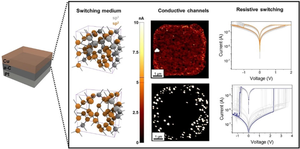
Physical observation of electrochemical metallization (ECM) channel is required for understanding the electrical characteristics of ECM memristors. Although numerous studies have explored to identify the ECM channels, the majority of approaches have been limited to in-situ systems and localized areas, lacking a comprehensive demonstration of their findings. This study focuses on interpreting the different electrical characteristics of ECM memristors through identification of ECM channels using a new method inspired by etch pit detection on Si surface for determining copper contamination. Atomic Force Microscopy (AFM), Scanning Electron Microscopy (SEM), and Transmission Electron Microscopy (TEM) were utilized to detect and analyze conductive channels within the switching medium after real operation. Interestingly, devices with insulating amorphous carbon (a-C) as medium layer exhibited multiple channels, while devices with semiconducting a-C layers showed a single channel in the on-state. Furthermore, devices with a single channel demonstrated more uniform switching parameters, including high resistance state and set voltage, compared to devices with multiple channels. However, devices with multiple channels exhibited better retention properties .In addition, intermetallic conductive channels were confirmed, resulting from the mixing of Cu active metal ions with the Pt bottom electrode in high current density conditions. The findings of this work provide valuable insights into interpreting ECM memristor performance based on the formation of channels and inspire device design strategies for improving device performance.
期刊介绍:
Electronic Materials Letters is an official journal of the Korean Institute of Metals and Materials. It is a peer-reviewed international journal publishing print and online version. It covers all disciplines of research and technology in electronic materials. Emphasis is placed on science, engineering and applications of advanced materials, including electronic, magnetic, optical, organic, electrochemical, mechanical, and nanoscale materials. The aspects of synthesis and processing include thin films, nanostructures, self assembly, and bulk, all related to thermodynamics, kinetics and/or modeling.


 分享
分享
 求助内容:
求助内容: 应助结果提醒方式:
 扫码关注我们
