Ting Wang, Songang Peng, Zhi Jin, Chen Hu, He Tian
{"title":"Interface Characterization of Graphene-Silicon Heterojunction Using Hg Probe Capacitance–Voltage Measurement","authors":"Ting Wang, Songang Peng, Zhi Jin, Chen Hu, He Tian","doi":"10.1002/admi.202400184","DOIUrl":null,"url":null,"abstract":"<p>Investigating the intrinsic properties of the Schottky interface between graphene and 3D bulk silicon is crucial. However, the semiconductor technology introduces extra doping and defects in graphene, which significantly disturbs the property of the graphene-silicon interface. Here, the interface parameters of graphene/n-Si heterojunction are derived by the damage-free Hg-probe capacitance–voltage measurement. Due to its low-density states, the Fermi level of graphene can be pushed upward, which results in a lower Schottky barrier height (<i>Φ<sub>B0</sub></i>) of Hg/graphene/n-Si (HGS) heterostructure than that of Hg/n-Si (HS) structure. Additionally, the series resistance (<i>R<sub>s</sub></i>) of HGS becomes lower than that of HS, which can be attributed to the narrowed depletion layer width (<i>W<sub>D</sub></i>) and the decreased interface state density (<i>N<sub>it</sub></i>). Furthermore, the frequency characteristic is also investigated. Because of the weak interface state charge trapping–detrapping process and the decreased <i>N<sub>it</sub></i> at high frequency, electrons will accumulate in graphene, and the Fermi level will be pushed up. Hence, the <i>Φ<sub>B0</sub></i> and <i>R<sub>s</sub></i> will decrease with increasing frequency. This study contributes to a deep understanding of the graphene/silicon heterojunction interfaces, which is crucial for designing and optimizing the new electronic and optoelectronic devices based on 2D/3D heterostructure.</p>","PeriodicalId":115,"journal":{"name":"Advanced Materials Interfaces","volume":"11 23","pages":""},"PeriodicalIF":4.4000,"publicationDate":"2024-07-08","publicationTypes":"Journal Article","fieldsOfStudy":null,"isOpenAccess":false,"openAccessPdf":"https://onlinelibrary.wiley.com/doi/epdf/10.1002/admi.202400184","citationCount":"0","resultStr":null,"platform":"Semanticscholar","paperid":null,"PeriodicalName":"Advanced Materials Interfaces","FirstCategoryId":"88","ListUrlMain":"https://advanced.onlinelibrary.wiley.com/doi/10.1002/admi.202400184","RegionNum":3,"RegionCategory":"材料科学","ArticlePicture":[],"TitleCN":null,"AbstractTextCN":null,"PMCID":null,"EPubDate":"","PubModel":"","JCR":"Q2","JCRName":"CHEMISTRY, MULTIDISCIPLINARY","Score":null,"Total":0}
引用次数: 0
Abstract
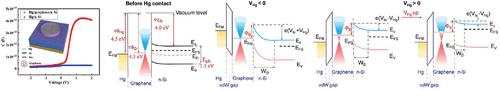
Investigating the intrinsic properties of the Schottky interface between graphene and 3D bulk silicon is crucial. However, the semiconductor technology introduces extra doping and defects in graphene, which significantly disturbs the property of the graphene-silicon interface. Here, the interface parameters of graphene/n-Si heterojunction are derived by the damage-free Hg-probe capacitance–voltage measurement. Due to its low-density states, the Fermi level of graphene can be pushed upward, which results in a lower Schottky barrier height (ΦB0) of Hg/graphene/n-Si (HGS) heterostructure than that of Hg/n-Si (HS) structure. Additionally, the series resistance (Rs) of HGS becomes lower than that of HS, which can be attributed to the narrowed depletion layer width (WD) and the decreased interface state density (Nit). Furthermore, the frequency characteristic is also investigated. Because of the weak interface state charge trapping–detrapping process and the decreased Nit at high frequency, electrons will accumulate in graphene, and the Fermi level will be pushed up. Hence, the ΦB0 and Rs will decrease with increasing frequency. This study contributes to a deep understanding of the graphene/silicon heterojunction interfaces, which is crucial for designing and optimizing the new electronic and optoelectronic devices based on 2D/3D heterostructure.
期刊介绍:
Advanced Materials Interfaces publishes top-level research on interface technologies and effects. Considering any interface formed between solids, liquids, and gases, the journal ensures an interdisciplinary blend of physics, chemistry, materials science, and life sciences. Advanced Materials Interfaces was launched in 2014 and received an Impact Factor of 4.834 in 2018.
The scope of Advanced Materials Interfaces is dedicated to interfaces and surfaces that play an essential role in virtually all materials and devices. Physics, chemistry, materials science and life sciences blend to encourage new, cross-pollinating ideas, which will drive forward our understanding of the processes at the interface.
Advanced Materials Interfaces covers all topics in interface-related research:
Oil / water separation,
Applications of nanostructured materials,
2D materials and heterostructures,
Surfaces and interfaces in organic electronic devices,
Catalysis and membranes,
Self-assembly and nanopatterned surfaces,
Composite and coating materials,
Biointerfaces for technical and medical applications.
Advanced Materials Interfaces provides a forum for topics on surface and interface science with a wide choice of formats: Reviews, Full Papers, and Communications, as well as Progress Reports and Research News.


 分享
分享
 求助内容:
求助内容: 应助结果提醒方式:
 扫码关注我们
