Julia Jagosz, Leander Willeke, Nils Gerke, Malte J. M. J. Becher, Paul Plate, Aleksander Kostka, Detlef Rogalla, Andreas Ostendorf, Claudia Bock
{"title":"Wafer-Scale Demonstration of Polycrystalline MoS2 Growth on 200 mm Glass and SiO2/Si Substrates by Plasma-Enhanced Atomic Layer Deposition","authors":"Julia Jagosz, Leander Willeke, Nils Gerke, Malte J. M. J. Becher, Paul Plate, Aleksander Kostka, Detlef Rogalla, Andreas Ostendorf, Claudia Bock","doi":"10.1002/admt.202400492","DOIUrl":null,"url":null,"abstract":"<p>2D materials like transition metal dichalcogenides (TMDCs) have been widely studied and are a gateway to modern technologies. While research today is mostly carried out on a laboratory scale, there is an intensive need for reliable processes on a wafer-scale, starting with monolayer-precise deposition of high-quality films. In this work, a plasma-enhanced atomic layer deposition (PEALD) process is developed on a 200 mm SiO<sub>2</sub>/Si substrate. The layers are investigated regarding crystallinity, composition, homogeneity, microstructure, topography, and electrical properties. The process is then applied on 200 mm alkali-free glass wafers aiming toward flexible electronics and compatibility with Si processes. A complete coverage of the wafer with a satisfying uniformity is achieved on both substrates and direct polycrystalline growth of MoS<sub>2</sub> films is verified on the entire wafer at a substrate temperature of <i>T </i>= 230 °C. On glass, the deposited MoS<sub>2</sub> films exhibit a higher crystallinity and are more planar compared to the SiO<sub>2</sub>/Si substrate. Furthermore, application relevant few-nanometer thick layers are investigated in detail. This low-temperature process inspires optimism for future direct integration of 2D-materials in an economical bottom-up approach on a wide variety of substrates, thus paving the way for industrial mass production.</p>","PeriodicalId":7292,"journal":{"name":"Advanced Materials Technologies","volume":"9 22","pages":""},"PeriodicalIF":6.4000,"publicationDate":"2024-07-12","publicationTypes":"Journal Article","fieldsOfStudy":null,"isOpenAccess":false,"openAccessPdf":"https://onlinelibrary.wiley.com/doi/epdf/10.1002/admt.202400492","citationCount":"0","resultStr":null,"platform":"Semanticscholar","paperid":null,"PeriodicalName":"Advanced Materials Technologies","FirstCategoryId":"88","ListUrlMain":"https://advanced.onlinelibrary.wiley.com/doi/10.1002/admt.202400492","RegionNum":3,"RegionCategory":"材料科学","ArticlePicture":[],"TitleCN":null,"AbstractTextCN":null,"PMCID":null,"EPubDate":"","PubModel":"","JCR":"Q1","JCRName":"MATERIALS SCIENCE, MULTIDISCIPLINARY","Score":null,"Total":0}
引用次数: 0
Abstract
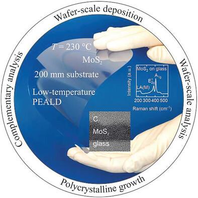
2D materials like transition metal dichalcogenides (TMDCs) have been widely studied and are a gateway to modern technologies. While research today is mostly carried out on a laboratory scale, there is an intensive need for reliable processes on a wafer-scale, starting with monolayer-precise deposition of high-quality films. In this work, a plasma-enhanced atomic layer deposition (PEALD) process is developed on a 200 mm SiO2/Si substrate. The layers are investigated regarding crystallinity, composition, homogeneity, microstructure, topography, and electrical properties. The process is then applied on 200 mm alkali-free glass wafers aiming toward flexible electronics and compatibility with Si processes. A complete coverage of the wafer with a satisfying uniformity is achieved on both substrates and direct polycrystalline growth of MoS2 films is verified on the entire wafer at a substrate temperature of T = 230 °C. On glass, the deposited MoS2 films exhibit a higher crystallinity and are more planar compared to the SiO2/Si substrate. Furthermore, application relevant few-nanometer thick layers are investigated in detail. This low-temperature process inspires optimism for future direct integration of 2D-materials in an economical bottom-up approach on a wide variety of substrates, thus paving the way for industrial mass production.
期刊介绍:
Advanced Materials Technologies Advanced Materials Technologies is the new home for all technology-related materials applications research, with particular focus on advanced device design, fabrication and integration, as well as new technologies based on novel materials. It bridges the gap between fundamental laboratory research and industry.


 分享
分享
 求助内容:
求助内容: 应助结果提醒方式:
 扫码关注我们
