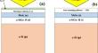
{"title":"Simulation of a-SiGe/c-Si solar cell with silicene front contact","authors":"Kiarash Madmeli, Arash Madmeli, Jabbar Ganji","doi":"10.1007/s11082-024-07225-6","DOIUrl":null,"url":null,"abstract":"<p>The objective of the present study was to utilize the two-dimensional (2D) structures of silicone (known as silicene) in the structure of solar cells. Its spectacular optical and electronic properties justify its application in solar structures. For this purpose, silicene was involved in the solar cell structure in 3 manners: as silicene1, an n-type semiconductor layer doped with P impurity; silicene2, a p-type semiconductor layer doped with Al; and as the free-standing silicene for the front contact. The former two applications were conducted in the ITO/silicene (1, 2)/<span>\\(\\textrm{MoS}_2\\)</span> (n)/a-SiGe: H (i)/c-Si (P)/Au structure, while the latter was in the Silicene/<span>\\(\\textrm{MoS}_2\\)</span> (n)/a-SiGe: H (i)/c-Si (P)/Au structure. Using the AFORS-HET software, the solar cells were exposed to AM1.5 spectrum radiation at 300 K temperature, and the impacts of 1 sun, 0.1 sun, and 10 sun illumination intensities were evaluated to obtain a better insight into the function of this 2D structure. The highest efficiencies in the mentioned illumination intensities were observed in the proposed cell with the silicene1 layer as the semiconductor, which were 18.96, 17.96, and 19.22%, respectively. Moreover, the efficiencies of the cell with free-standing silicene as the front contact were 27.13, 25.95, and 27.65%, respectively, in the mentioned illumination intensities.</p>","PeriodicalId":720,"journal":{"name":"Optical and Quantum Electronics","volume":"41 1","pages":""},"PeriodicalIF":4.0000,"publicationDate":"2024-09-05","publicationTypes":"Journal Article","fieldsOfStudy":null,"isOpenAccess":false,"openAccessPdf":"","citationCount":"0","resultStr":null,"platform":"Semanticscholar","paperid":null,"PeriodicalName":"Optical and Quantum Electronics","FirstCategoryId":"5","ListUrlMain":"https://doi.org/10.1007/s11082-024-07225-6","RegionNum":3,"RegionCategory":"工程技术","ArticlePicture":[],"TitleCN":null,"AbstractTextCN":null,"PMCID":null,"EPubDate":"","PubModel":"","JCR":"Q2","JCRName":"ENGINEERING, ELECTRICAL & ELECTRONIC","Score":null,"Total":0}
引用次数: 0
Abstract
The objective of the present study was to utilize the two-dimensional (2D) structures of silicone (known as silicene) in the structure of solar cells. Its spectacular optical and electronic properties justify its application in solar structures. For this purpose, silicene was involved in the solar cell structure in 3 manners: as silicene1, an n-type semiconductor layer doped with P impurity; silicene2, a p-type semiconductor layer doped with Al; and as the free-standing silicene for the front contact. The former two applications were conducted in the ITO/silicene (1, 2)/\(\textrm{MoS}_2\) (n)/a-SiGe: H (i)/c-Si (P)/Au structure, while the latter was in the Silicene/\(\textrm{MoS}_2\) (n)/a-SiGe: H (i)/c-Si (P)/Au structure. Using the AFORS-HET software, the solar cells were exposed to AM1.5 spectrum radiation at 300 K temperature, and the impacts of 1 sun, 0.1 sun, and 10 sun illumination intensities were evaluated to obtain a better insight into the function of this 2D structure. The highest efficiencies in the mentioned illumination intensities were observed in the proposed cell with the silicene1 layer as the semiconductor, which were 18.96, 17.96, and 19.22%, respectively. Moreover, the efficiencies of the cell with free-standing silicene as the front contact were 27.13, 25.95, and 27.65%, respectively, in the mentioned illumination intensities.
期刊介绍:
Optical and Quantum Electronics provides an international forum for the publication of original research papers, tutorial reviews and letters in such fields as optical physics, optical engineering and optoelectronics. Special issues are published on topics of current interest.
Optical and Quantum Electronics is published monthly. It is concerned with the technology and physics of optical systems, components and devices, i.e., with topics such as: optical fibres; semiconductor lasers and LEDs; light detection and imaging devices; nanophotonics; photonic integration and optoelectronic integrated circuits; silicon photonics; displays; optical communications from devices to systems; materials for photonics (e.g. semiconductors, glasses, graphene); the physics and simulation of optical devices and systems; nanotechnologies in photonics (including engineered nano-structures such as photonic crystals, sub-wavelength photonic structures, metamaterials, and plasmonics); advanced quantum and optoelectronic applications (e.g. quantum computing, memory and communications, quantum sensing and quantum dots); photonic sensors and bio-sensors; Terahertz phenomena; non-linear optics and ultrafast phenomena; green photonics.


 分享
分享
 求助内容:
求助内容: 应助结果提醒方式:
 扫码关注我们
