K. E. Ivlev, V. V. Bolotov, I. V. Ponomareva, E. V. Knyazev
{"title":"Formation of Channel Silicon to Create Filter Layers","authors":"K. E. Ivlev, V. V. Bolotov, I. V. Ponomareva, E. V. Knyazev","doi":"10.1134/s1063782624030060","DOIUrl":null,"url":null,"abstract":"<h3 data-test=\"abstract-sub-heading\">Abstract</h3><p>The features of the formation of porous layers on substrates of low doped silicon of и-type conductivity by anodic etching using illumination are considered. The formation of microporous silicon layer on the walls of macropores was found. It is shown that the illumination modes strongly influence the morphological parameters of the obtained layers. After exposure to alkali, macroporous layers with pore diameters up to 550 nm were obtained, which can be used to create filter layers.</p>","PeriodicalId":21760,"journal":{"name":"Semiconductors","volume":"32 1","pages":""},"PeriodicalIF":0.6000,"publicationDate":"2024-09-04","publicationTypes":"Journal Article","fieldsOfStudy":null,"isOpenAccess":false,"openAccessPdf":"","citationCount":"0","resultStr":null,"platform":"Semanticscholar","paperid":null,"PeriodicalName":"Semiconductors","FirstCategoryId":"101","ListUrlMain":"https://doi.org/10.1134/s1063782624030060","RegionNum":4,"RegionCategory":"物理与天体物理","ArticlePicture":[],"TitleCN":null,"AbstractTextCN":null,"PMCID":null,"EPubDate":"","PubModel":"","JCR":"Q4","JCRName":"PHYSICS, CONDENSED MATTER","Score":null,"Total":0}
引用次数: 0
Abstract
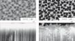
The features of the formation of porous layers on substrates of low doped silicon of и-type conductivity by anodic etching using illumination are considered. The formation of microporous silicon layer on the walls of macropores was found. It is shown that the illumination modes strongly influence the morphological parameters of the obtained layers. After exposure to alkali, macroporous layers with pore diameters up to 550 nm were obtained, which can be used to create filter layers.
期刊介绍:
Publishes the most important work in semiconductor research in the countries of the former Soviet Union. Covers semiconductor theory, transport phenomena in semiconductors, optics, magnetooptics, and electrooptics of semiconductors, semiconductor lasers and semiconductor surface physics. The journal features an extensive book review section.


 分享
分享
 求助内容:
求助内容: 应助结果提醒方式:
 扫码关注我们
