Juliane Koch, Patrick Häuser, Peter Kleinschmidt, Werner Prost, Nils Weimann, Thomas Hannappel
{"title":"Tracking Charge Carrier Paths in Freestanding GaN/AlN Nanowires on Si(111)","authors":"Juliane Koch, Patrick Häuser, Peter Kleinschmidt, Werner Prost, Nils Weimann, Thomas Hannappel","doi":"10.1021/acsami.4c10179","DOIUrl":null,"url":null,"abstract":"Functional and abundant substrate materials are relevant for applying all sophisticated semiconductor-based device components such as nanowire arrays. In the case of GaN nanowires grown by metalorganic vapor phase epitaxy, Si(111) substrates are widely used, together with an AlN interlayer to suppress the well-known Ga-based melt-back-etching. However, the AlN interlayer can degrade the interfacial conductivity of the Si(111) substrate. To reveal the possible impact of this interlayer on the overall electrical performance, an advanced analysis of the electrical behavior with suitable spatial resolution is essential. For the electrical investigation of the nanowire-to-substrate junction, we used a four-point probe measurement setup with sufficiently high spatial resolution. The charge separation behavior of the junction is also demonstrated by an electron beam-induced current mode, while the n-GaN nanowire (NW) core exhibits good electrical conductivity. The charge carrier-selective transport at the NW-to-substrate junction can be attributed to different, local material compositions by two main effects: the reduction of Ga adatoms by shadowing of the lower part of the NW structure by the top part during growth, i.e. the protection of the pedestal footprint from Ga adsorption. Our combination of investigation methods provides direct insight into the nanowire-to-substrate junction and leads to a model of the conductivity channels at the nanowire base. This knowledge is crucial for all future GaN bottom-up grown nanowire structure devices on conductive Si(111) substrates.","PeriodicalId":5,"journal":{"name":"ACS Applied Materials & Interfaces","volume":"141 1","pages":""},"PeriodicalIF":7.8000,"publicationDate":"2024-09-19","publicationTypes":"Journal Article","fieldsOfStudy":null,"isOpenAccess":false,"openAccessPdf":"","citationCount":"0","resultStr":null,"platform":"Semanticscholar","paperid":null,"PeriodicalName":"ACS Applied Materials & Interfaces","FirstCategoryId":"88","ListUrlMain":"https://doi.org/10.1021/acsami.4c10179","RegionNum":2,"RegionCategory":"材料科学","ArticlePicture":[],"TitleCN":null,"AbstractTextCN":null,"PMCID":null,"EPubDate":"","PubModel":"","JCR":"Q1","JCRName":"MATERIALS SCIENCE, MULTIDISCIPLINARY","Score":null,"Total":0}
引用次数: 0
Abstract
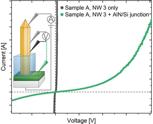
Functional and abundant substrate materials are relevant for applying all sophisticated semiconductor-based device components such as nanowire arrays. In the case of GaN nanowires grown by metalorganic vapor phase epitaxy, Si(111) substrates are widely used, together with an AlN interlayer to suppress the well-known Ga-based melt-back-etching. However, the AlN interlayer can degrade the interfacial conductivity of the Si(111) substrate. To reveal the possible impact of this interlayer on the overall electrical performance, an advanced analysis of the electrical behavior with suitable spatial resolution is essential. For the electrical investigation of the nanowire-to-substrate junction, we used a four-point probe measurement setup with sufficiently high spatial resolution. The charge separation behavior of the junction is also demonstrated by an electron beam-induced current mode, while the n-GaN nanowire (NW) core exhibits good electrical conductivity. The charge carrier-selective transport at the NW-to-substrate junction can be attributed to different, local material compositions by two main effects: the reduction of Ga adatoms by shadowing of the lower part of the NW structure by the top part during growth, i.e. the protection of the pedestal footprint from Ga adsorption. Our combination of investigation methods provides direct insight into the nanowire-to-substrate junction and leads to a model of the conductivity channels at the nanowire base. This knowledge is crucial for all future GaN bottom-up grown nanowire structure devices on conductive Si(111) substrates.
期刊介绍:
ACS Applied Materials & Interfaces is a leading interdisciplinary journal that brings together chemists, engineers, physicists, and biologists to explore the development and utilization of newly-discovered materials and interfacial processes for specific applications. Our journal has experienced remarkable growth since its establishment in 2009, both in terms of the number of articles published and the impact of the research showcased. We are proud to foster a truly global community, with the majority of published articles originating from outside the United States, reflecting the rapid growth of applied research worldwide.


 分享
分享
 求助内容:
求助内容: 应助结果提醒方式:
 扫码关注我们
