Yiyuan Sun, Ying Xu, Zijie Zheng, Yuxuan Wang, Yuye Kang, Kaizhen Han, Wei Shi, Jinyong Wang and Xiao Gong*,
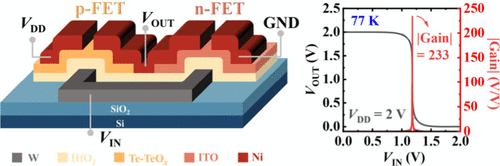
{"title":"BEOL Three-Dimensional Stackable Oxide Semiconductor CMOS Inverter with a High Voltage Gain of 233 at Cryogenic Temperatures","authors":"Yiyuan Sun, Ying Xu, Zijie Zheng, Yuxuan Wang, Yuye Kang, Kaizhen Han, Wei Shi, Jinyong Wang and Xiao Gong*, ","doi":"10.1021/acs.nanolett.4c04701","DOIUrl":null,"url":null,"abstract":"<p >Targeting high-performance computing at cryogenic temperatures, we report back-end-of-line (BEOL)-compatible p-type Te-TeO<sub><i>x</i></sub> field effect transistors (FETs) deposited using a sputtering method that is cost-effective, large-scale manufacturable, and highly controllable. Combined with the indium tin oxide channel n-FETs employing a common gate and HfO<sub>2</sub> gate dielectric, BEOL three-dimensional stackable oxide semiconductor complementary metal oxide semiconductor (CMOS) inverters were further realized, demonstrating excellent threshold voltage matching, with a high voltage gain of 132 with a 2 V supply voltage (<i>V</i><sub>DD</sub>) at room temperature. At cryogenic temperatures, the CMOS inverter exhibits significantly enhanced performance, achieving a voltage gain of 233 at a <i>V</i><sub>DD</sub> of 2 V with a wide noise margin of 86%. Even at an ultralow <i>V</i><sub>DD</sub> of 0.5 V, the CMOS inverter maintains solid performance with an exceptionally low power consumption of <60 pW.</p>","PeriodicalId":53,"journal":{"name":"Nano Letters","volume":"25 31","pages":"11757–11761"},"PeriodicalIF":9.1000,"publicationDate":"2024-12-20","publicationTypes":"Journal Article","fieldsOfStudy":null,"isOpenAccess":false,"openAccessPdf":"","citationCount":"0","resultStr":null,"platform":"Semanticscholar","paperid":null,"PeriodicalName":"Nano Letters","FirstCategoryId":"88","ListUrlMain":"https://pubs.acs.org/doi/10.1021/acs.nanolett.4c04701","RegionNum":1,"RegionCategory":"材料科学","ArticlePicture":[],"TitleCN":null,"AbstractTextCN":null,"PMCID":null,"EPubDate":"","PubModel":"","JCR":"Q1","JCRName":"CHEMISTRY, MULTIDISCIPLINARY","Score":null,"Total":0}
引用次数: 0
Abstract
Targeting high-performance computing at cryogenic temperatures, we report back-end-of-line (BEOL)-compatible p-type Te-TeOx field effect transistors (FETs) deposited using a sputtering method that is cost-effective, large-scale manufacturable, and highly controllable. Combined with the indium tin oxide channel n-FETs employing a common gate and HfO2 gate dielectric, BEOL three-dimensional stackable oxide semiconductor complementary metal oxide semiconductor (CMOS) inverters were further realized, demonstrating excellent threshold voltage matching, with a high voltage gain of 132 with a 2 V supply voltage (VDD) at room temperature. At cryogenic temperatures, the CMOS inverter exhibits significantly enhanced performance, achieving a voltage gain of 233 at a VDD of 2 V with a wide noise margin of 86%. Even at an ultralow VDD of 0.5 V, the CMOS inverter maintains solid performance with an exceptionally low power consumption of <60 pW.
期刊介绍:
Nano Letters serves as a dynamic platform for promptly disseminating original results in fundamental, applied, and emerging research across all facets of nanoscience and nanotechnology. A pivotal criterion for inclusion within Nano Letters is the convergence of at least two different areas or disciplines, ensuring a rich interdisciplinary scope. The journal is dedicated to fostering exploration in diverse areas, including:
- Experimental and theoretical findings on physical, chemical, and biological phenomena at the nanoscale
- Synthesis, characterization, and processing of organic, inorganic, polymer, and hybrid nanomaterials through physical, chemical, and biological methodologies
- Modeling and simulation of synthetic, assembly, and interaction processes
- Realization of integrated nanostructures and nano-engineered devices exhibiting advanced performance
- Applications of nanoscale materials in living and environmental systems
Nano Letters is committed to advancing and showcasing groundbreaking research that intersects various domains, fostering innovation and collaboration in the ever-evolving field of nanoscience and nanotechnology.


 分享
分享
 求助内容:
求助内容: 应助结果提醒方式:
 扫码关注我们
