Zejun Ye, Zengxin Yan, Xinliang Guo, Yang Yang, Jiaming Sun
{"title":"Interface Modification by Ga2O3 Atomic Layers within Er-Doped GeO2 Nanofilms for Enhanced Electroluminescence and Operation Stability","authors":"Zejun Ye, Zengxin Yan, Xinliang Guo, Yang Yang, Jiaming Sun","doi":"10.1021/acsami.4c15787","DOIUrl":null,"url":null,"abstract":"For silicon-based devices using dielectric oxides doped with rare earth ions, their electroluminescence (EL) performance relies on the sufficient carrier injection. In this work, the atomic Ga<sub>2</sub>O<sub>3</sub> layers are inserted within the Er-doped GeO<sub>2</sub> nanofilms fabricated by atomic layer deposition (ALD). Both Ga(CH<sub>3</sub>)<sub>3</sub> and Ga(C<sub>2</sub>H<sub>5</sub>)<sub>3</sub> could realize the ALD growth of Ga<sub>2</sub>O<sub>3</sub> onto the as-deposited GeO<sub>2</sub> nanofilm with unaffected deposition rates. The interfacial defects introduced by atomic Ga<sub>2</sub>O<sub>3</sub> layers decrease the threshold voltage while increasing the tolerable injection current of the EL devices; the 1530 nm emissions from the 600 °C-annealed Ga<sub>2</sub>O<sub>3</sub>/GeO<sub>2</sub>:Er nanolaminate devices achieve the optical power density of 16.2 mW/cm<sup>2</sup>, with the excitation efficiency increased to 12.5%. Moreover, the interface modification by atomic Ga<sub>2</sub>O<sub>3</sub> layers significantly prolongs the operation time of these prototype devices, reaching 5.21 × 10<sup>4</sup> s for the optimal one. High-temperature annealing above 800 °C results in the decomposition of GeO<sub>2</sub> and leaves reticular porous nanofilms. The conduction mode within these amorphous Ga<sub>2</sub>O<sub>3</sub>/GeO<sub>2</sub>:Er nanolaminates conforms to the trap-assisted tunneling mechanism, with the depths of defect states lowered by the interfacial Ga<sub>2</sub>O<sub>3</sub> layers. These Ga<sub>2</sub>O<sub>3</sub>/GeO<sub>2</sub>:Er nanolaminates with improved EL performance demonstrate new potential in the utilization of ALD GeO<sub>2</sub> nanofilms in silicon-compatible optoelectronics.","PeriodicalId":5,"journal":{"name":"ACS Applied Materials & Interfaces","volume":"16 1","pages":""},"PeriodicalIF":8.2000,"publicationDate":"2025-01-04","publicationTypes":"Journal Article","fieldsOfStudy":null,"isOpenAccess":false,"openAccessPdf":"","citationCount":"0","resultStr":null,"platform":"Semanticscholar","paperid":null,"PeriodicalName":"ACS Applied Materials & Interfaces","FirstCategoryId":"88","ListUrlMain":"https://doi.org/10.1021/acsami.4c15787","RegionNum":2,"RegionCategory":"材料科学","ArticlePicture":[],"TitleCN":null,"AbstractTextCN":null,"PMCID":null,"EPubDate":"","PubModel":"","JCR":"Q1","JCRName":"MATERIALS SCIENCE, MULTIDISCIPLINARY","Score":null,"Total":0}
引用次数: 0
Abstract
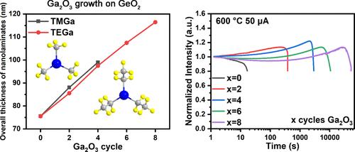
For silicon-based devices using dielectric oxides doped with rare earth ions, their electroluminescence (EL) performance relies on the sufficient carrier injection. In this work, the atomic Ga2O3 layers are inserted within the Er-doped GeO2 nanofilms fabricated by atomic layer deposition (ALD). Both Ga(CH3)3 and Ga(C2H5)3 could realize the ALD growth of Ga2O3 onto the as-deposited GeO2 nanofilm with unaffected deposition rates. The interfacial defects introduced by atomic Ga2O3 layers decrease the threshold voltage while increasing the tolerable injection current of the EL devices; the 1530 nm emissions from the 600 °C-annealed Ga2O3/GeO2:Er nanolaminate devices achieve the optical power density of 16.2 mW/cm2, with the excitation efficiency increased to 12.5%. Moreover, the interface modification by atomic Ga2O3 layers significantly prolongs the operation time of these prototype devices, reaching 5.21 × 10⁴ s for the optimal one. High-temperature annealing above 800 °C results in the decomposition of GeO2 and leaves reticular porous nanofilms. The conduction mode within these amorphous Ga2O3/GeO2:Er nanolaminates conforms to the trap-assisted tunneling mechanism, with the depths of defect states lowered by the interfacial Ga2O3 layers. These Ga2O3/GeO2:Er nanolaminates with improved EL performance demonstrate new potential in the utilization of ALD GeO2 nanofilms in silicon-compatible optoelectronics.
期刊介绍:
ACS Applied Materials & Interfaces is a leading interdisciplinary journal that brings together chemists, engineers, physicists, and biologists to explore the development and utilization of newly-discovered materials and interfacial processes for specific applications. Our journal has experienced remarkable growth since its establishment in 2009, both in terms of the number of articles published and the impact of the research showcased. We are proud to foster a truly global community, with the majority of published articles originating from outside the United States, reflecting the rapid growth of applied research worldwide.


 分享
分享
 求助内容:
求助内容: 应助结果提醒方式:
 扫码关注我们
