Seonwoong Jung , Dongmin Yoon , Seokmin Oh, Hyerin Shin, Jungwoo Kim, Dae-Hong Ko
{"title":"Study on the interfaces between Si and SiGe in the epitaxial in-situ Boron-Doped SiGe/Si layers treated with H or Cl","authors":"Seonwoong Jung , Dongmin Yoon , Seokmin Oh, Hyerin Shin, Jungwoo Kim, Dae-Hong Ko","doi":"10.1016/j.apsusc.2025.162553","DOIUrl":null,"url":null,"abstract":"<div><div>Abrupt interfaces in alternating SiGe/Si epitaxial layers are critical for vertically stacked devices. Formation of broad interfaces during the epitaxial growth can lead to variations in the surfaces and the thicknesses of Si channels upon subsequent SiGe selective etching, which result in the degradation of the device performance. This study focuses on a detailed interface analysis of the <em>in-situ</em> B-doped SiGe/Si epitaxial layers under H or Cl surface treatment during the epitaxial growth. In our study, surface treatments using H or Cl species are applied on SiGe surfaces prior to the Si layer growth to modify the surface bond energies at the initial epitaxial growth of Si on SiGe. High-resolution transmission electron microscopy provides direct evidence of broad interfaces with an increase in B concentration, whereas H- or Cl-terminated SiGe surfaces limit Ge surface segregation, leading to the formation of epitaxial structures with abrupt and well-defined interfaces. Our results provide a comprehensive understanding of how B concentration and surface treatments can control the interfacial properties of SiGe/Si structure, providing the process for the optimized multilayer structures in the vertically stacked device fabrications.</div></div>","PeriodicalId":247,"journal":{"name":"Applied Surface Science","volume":"690 ","pages":"Article 162553"},"PeriodicalIF":6.9000,"publicationDate":"2025-05-01","publicationTypes":"Journal Article","fieldsOfStudy":null,"isOpenAccess":false,"openAccessPdf":"","citationCount":"0","resultStr":null,"platform":"Semanticscholar","paperid":null,"PeriodicalName":"Applied Surface Science","FirstCategoryId":"88","ListUrlMain":"https://www.sciencedirect.com/science/article/pii/S0169433225002673","RegionNum":2,"RegionCategory":"材料科学","ArticlePicture":[],"TitleCN":null,"AbstractTextCN":null,"PMCID":null,"EPubDate":"2025/1/30 0:00:00","PubModel":"Epub","JCR":"Q2","JCRName":"CHEMISTRY, PHYSICAL","Score":null,"Total":0}
引用次数: 0
Abstract
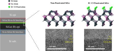
Abrupt interfaces in alternating SiGe/Si epitaxial layers are critical for vertically stacked devices. Formation of broad interfaces during the epitaxial growth can lead to variations in the surfaces and the thicknesses of Si channels upon subsequent SiGe selective etching, which result in the degradation of the device performance. This study focuses on a detailed interface analysis of the in-situ B-doped SiGe/Si epitaxial layers under H or Cl surface treatment during the epitaxial growth. In our study, surface treatments using H or Cl species are applied on SiGe surfaces prior to the Si layer growth to modify the surface bond energies at the initial epitaxial growth of Si on SiGe. High-resolution transmission electron microscopy provides direct evidence of broad interfaces with an increase in B concentration, whereas H- or Cl-terminated SiGe surfaces limit Ge surface segregation, leading to the formation of epitaxial structures with abrupt and well-defined interfaces. Our results provide a comprehensive understanding of how B concentration and surface treatments can control the interfacial properties of SiGe/Si structure, providing the process for the optimized multilayer structures in the vertically stacked device fabrications.
期刊介绍:
Applied Surface Science covers topics contributing to a better understanding of surfaces, interfaces, nanostructures and their applications. The journal is concerned with scientific research on the atomic and molecular level of material properties determined with specific surface analytical techniques and/or computational methods, as well as the processing of such structures.


 分享
分享
 求助内容:
求助内容: 应助结果提醒方式:
 扫码关注我们
