Yuanqiu Tan, Shao-Heng Yang, Chih-Pin Lin, Fernando J. Vega, Jun Cai, Hao-Yu Lan, Rahul Tripathi, Sahej Sharma, Zhongxia Shang, Tuo-Hung Hou, Thomas E. Beechem, Joerg Appenzeller, Zhihong Chen
{"title":"Monolayer WSe2 Field-Effect Transistor Performance Enhancement by Atomic Defect Engineering and Passivation","authors":"Yuanqiu Tan, Shao-Heng Yang, Chih-Pin Lin, Fernando J. Vega, Jun Cai, Hao-Yu Lan, Rahul Tripathi, Sahej Sharma, Zhongxia Shang, Tuo-Hung Hou, Thomas E. Beechem, Joerg Appenzeller, Zhihong Chen","doi":"10.1021/acsnano.4c16831","DOIUrl":null,"url":null,"abstract":"Monolayer two-dimensional (2D) transition metal dichalcogenides (TMDs) have emerged as leading candidates for next-generation electronic devices beyond silicon, owing to their atomically thin structure and superior electrostatic control. However, their integration into industrial applications remains limited due to high densities of lattice defects and challenges in achieving stable and effective doping. In this work, we present a passivation and doping technique that significantly recovers and enhances the electrical properties of monolayer tungsten diselenide (WSe<sub>2</sub>). Our defect-facilitated (NH<sub>4</sub>)<sub>2</sub>S surface passivation approach has achieved robust enhancements in both the on-state and off-state performance of monolayer WSe<sub>2</sub> p-type field-effect transistors (p-FETs), enhancing channel mobility 3-fold, reaching a subthreshold slope (<i>SS</i><sub>min</sub>) value of 70 mV/dec, on-currents of 110 μA/μm, and <i>I</i><sub>max</sub>/<i>I</i><sub>min</sub> > 10<sup>9</sup>, while maintaining stability across a range of conditions. Furthermore, we establish a strong correlation between device off-state performance and the full width at half-maximum (fwhm) of the Raman characterization peak. The defect engineering approach, combined with (NH<sub>4</sub>)<sub>2</sub>S treatment at room temperature, offers a viable pathway for passivation and substitutional doping, advancing the potential for improved charge transport in future 2D TMD-based electronic devices.","PeriodicalId":21,"journal":{"name":"ACS Nano","volume":"70 1","pages":""},"PeriodicalIF":16.0000,"publicationDate":"2025-02-27","publicationTypes":"Journal Article","fieldsOfStudy":null,"isOpenAccess":false,"openAccessPdf":"","citationCount":"0","resultStr":null,"platform":"Semanticscholar","paperid":null,"PeriodicalName":"ACS Nano","FirstCategoryId":"88","ListUrlMain":"https://doi.org/10.1021/acsnano.4c16831","RegionNum":1,"RegionCategory":"材料科学","ArticlePicture":[],"TitleCN":null,"AbstractTextCN":null,"PMCID":null,"EPubDate":"","PubModel":"","JCR":"Q1","JCRName":"CHEMISTRY, MULTIDISCIPLINARY","Score":null,"Total":0}
引用次数: 0
Abstract
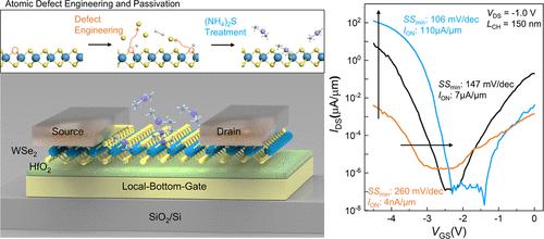
Monolayer two-dimensional (2D) transition metal dichalcogenides (TMDs) have emerged as leading candidates for next-generation electronic devices beyond silicon, owing to their atomically thin structure and superior electrostatic control. However, their integration into industrial applications remains limited due to high densities of lattice defects and challenges in achieving stable and effective doping. In this work, we present a passivation and doping technique that significantly recovers and enhances the electrical properties of monolayer tungsten diselenide (WSe2). Our defect-facilitated (NH4)2S surface passivation approach has achieved robust enhancements in both the on-state and off-state performance of monolayer WSe2 p-type field-effect transistors (p-FETs), enhancing channel mobility 3-fold, reaching a subthreshold slope (SSmin) value of 70 mV/dec, on-currents of 110 μA/μm, and Imax/Imin > 109, while maintaining stability across a range of conditions. Furthermore, we establish a strong correlation between device off-state performance and the full width at half-maximum (fwhm) of the Raman characterization peak. The defect engineering approach, combined with (NH4)2S treatment at room temperature, offers a viable pathway for passivation and substitutional doping, advancing the potential for improved charge transport in future 2D TMD-based electronic devices.
期刊介绍:
ACS Nano, published monthly, serves as an international forum for comprehensive articles on nanoscience and nanotechnology research at the intersections of chemistry, biology, materials science, physics, and engineering. The journal fosters communication among scientists in these communities, facilitating collaboration, new research opportunities, and advancements through discoveries. ACS Nano covers synthesis, assembly, characterization, theory, and simulation of nanostructures, nanobiotechnology, nanofabrication, methods and tools for nanoscience and nanotechnology, and self- and directed-assembly. Alongside original research articles, it offers thorough reviews, perspectives on cutting-edge research, and discussions envisioning the future of nanoscience and nanotechnology.


 分享
分享
 求助内容:
求助内容: 应助结果提醒方式:
 扫码关注我们
