Taisei Kano, Hiroyuki Nishinaka, Yuta Arata, Masahiro Yoshimoto
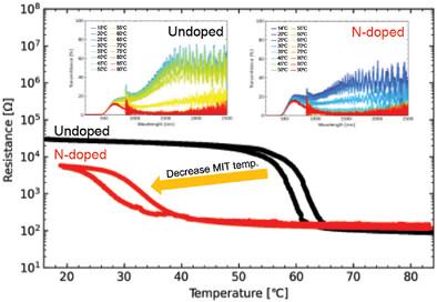
{"title":"通过喷雾化学气相沉积在合成云母基底上的 VO2 薄膜中掺氮:降低金属-绝缘体转变温度,实现智能窗口","authors":"Taisei Kano, Hiroyuki Nishinaka, Yuta Arata, Masahiro Yoshimoto","doi":"10.1002/admi.202400038","DOIUrl":null,"url":null,"abstract":"In this study, nitrogen (N) is doped into VO<jats:sub>2</jats:sub> thin films through mist chemical vapor deposition (CVD), and the effect of the doping on metal–insulator transition (MIT) temperatures is investigated. The N‐doped VO<jats:sub>2</jats:sub> thin films are grown on an SnO<jats:sub>2</jats:sub> buffer layer. The N‐doped VO<jats:sub>2</jats:sub> lattice spacing tends to expand as the growth temperature decreased, which indicates that the incorporation of N into the lattice is derived from the Ethylenediamine. Secondary ion mass spectrometry (SIMS) is conducted to investigate the relationship between the decrease in the transition temperature and N concentration. The results reveal that the sample grown at 425 °C contains approximately 2 × 10<jats:sup>20</jats:sup> cm<jats:sup>−3</jats:sup> of N. Thus, efficient nitrogen doping can be achieved through mist CVD. The temperature‐resistance characteristics of VO<jats:sub>2</jats:sub> thin films are measured to investigate their electrical properties and MIT temperatures. The results reveal that for undoped samples, the transition temperature slightly decreases with the decrease in the growth temperature. Furthermore, the sample grown at 425 °C exhibits a considerable change in resistance because of MIT at approximately 29.5 °C. These results prove the potential of using mist CVD N‐doped thin films for smart window applications to address future energy problems.","PeriodicalId":115,"journal":{"name":"Advanced Materials Interfaces","volume":null,"pages":null},"PeriodicalIF":4.3000,"publicationDate":"2024-04-26","publicationTypes":"Journal Article","fieldsOfStudy":null,"isOpenAccess":false,"openAccessPdf":"","citationCount":"0","resultStr":"{\"title\":\"Nitrogen Doping in VO2 Thin Films on Synthetic Mica Substrates Through Mist Chemical Vapor Deposition: Lowering the Metal–Insulator Transition Temperature Toward Smart Windows\",\"authors\":\"Taisei Kano, Hiroyuki Nishinaka, Yuta Arata, Masahiro Yoshimoto\",\"doi\":\"10.1002/admi.202400038\",\"DOIUrl\":null,\"url\":null,\"abstract\":\"In this study, nitrogen (N) is doped into VO<jats:sub>2</jats:sub> thin films through mist chemical vapor deposition (CVD), and the effect of the doping on metal–insulator transition (MIT) temperatures is investigated. The N‐doped VO<jats:sub>2</jats:sub> thin films are grown on an SnO<jats:sub>2</jats:sub> buffer layer. The N‐doped VO<jats:sub>2</jats:sub> lattice spacing tends to expand as the growth temperature decreased, which indicates that the incorporation of N into the lattice is derived from the Ethylenediamine. Secondary ion mass spectrometry (SIMS) is conducted to investigate the relationship between the decrease in the transition temperature and N concentration. The results reveal that the sample grown at 425 °C contains approximately 2 × 10<jats:sup>20</jats:sup> cm<jats:sup>−3</jats:sup> of N. Thus, efficient nitrogen doping can be achieved through mist CVD. The temperature‐resistance characteristics of VO<jats:sub>2</jats:sub> thin films are measured to investigate their electrical properties and MIT temperatures. The results reveal that for undoped samples, the transition temperature slightly decreases with the decrease in the growth temperature. Furthermore, the sample grown at 425 °C exhibits a considerable change in resistance because of MIT at approximately 29.5 °C. These results prove the potential of using mist CVD N‐doped thin films for smart window applications to address future energy problems.\",\"PeriodicalId\":115,\"journal\":{\"name\":\"Advanced Materials Interfaces\",\"volume\":null,\"pages\":null},\"PeriodicalIF\":4.3000,\"publicationDate\":\"2024-04-26\",\"publicationTypes\":\"Journal Article\",\"fieldsOfStudy\":null,\"isOpenAccess\":false,\"openAccessPdf\":\"\",\"citationCount\":\"0\",\"resultStr\":null,\"platform\":\"Semanticscholar\",\"paperid\":null,\"PeriodicalName\":\"Advanced Materials Interfaces\",\"FirstCategoryId\":\"88\",\"ListUrlMain\":\"https://doi.org/10.1002/admi.202400038\",\"RegionNum\":3,\"RegionCategory\":\"材料科学\",\"ArticlePicture\":[],\"TitleCN\":null,\"AbstractTextCN\":null,\"PMCID\":null,\"EPubDate\":\"\",\"PubModel\":\"\",\"JCR\":\"Q2\",\"JCRName\":\"CHEMISTRY, MULTIDISCIPLINARY\",\"Score\":null,\"Total\":0}","platform":"Semanticscholar","paperid":null,"PeriodicalName":"Advanced Materials Interfaces","FirstCategoryId":"88","ListUrlMain":"https://doi.org/10.1002/admi.202400038","RegionNum":3,"RegionCategory":"材料科学","ArticlePicture":[],"TitleCN":null,"AbstractTextCN":null,"PMCID":null,"EPubDate":"","PubModel":"","JCR":"Q2","JCRName":"CHEMISTRY, MULTIDISCIPLINARY","Score":null,"Total":0}
引用次数: 0
摘要
本研究通过雾化化学气相沉积(CVD)将氮(N)掺杂到 VO2 薄膜中,并研究了掺杂对金属-绝缘体转变(MIT)温度的影响。掺杂 N 的 VO2 薄膜生长在 SnO2 缓冲层上。随着生长温度的降低,掺 N 的 VO2 晶格间距趋于扩大,这表明 N 在晶格中的掺入来自乙二胺。二次离子质谱法(SIMS)用于研究转变温度的降低与 N 浓度之间的关系。结果表明,在 425 °C 生长的样品含有约 2 × 1020 cm-3 的 N。测量了 VO2 薄膜的温度-电阻特性,以研究其电气特性和 MIT 温度。结果表明,对于未掺杂的样品,转变温度随着生长温度的降低而略有降低。此外,生长温度为 425 ℃ 的样品在大约 29.5 ℃ 时会出现 MIT,从而导致电阻发生显著变化。这些结果证明了将雾状 CVD 掺杂 N 薄膜用于智能窗应用以解决未来能源问题的潜力。
Nitrogen Doping in VO2 Thin Films on Synthetic Mica Substrates Through Mist Chemical Vapor Deposition: Lowering the Metal–Insulator Transition Temperature Toward Smart Windows
In this study, nitrogen (N) is doped into VO2 thin films through mist chemical vapor deposition (CVD), and the effect of the doping on metal–insulator transition (MIT) temperatures is investigated. The N‐doped VO2 thin films are grown on an SnO2 buffer layer. The N‐doped VO2 lattice spacing tends to expand as the growth temperature decreased, which indicates that the incorporation of N into the lattice is derived from the Ethylenediamine. Secondary ion mass spectrometry (SIMS) is conducted to investigate the relationship between the decrease in the transition temperature and N concentration. The results reveal that the sample grown at 425 °C contains approximately 2 × 1020 cm−3 of N. Thus, efficient nitrogen doping can be achieved through mist CVD. The temperature‐resistance characteristics of VO2 thin films are measured to investigate their electrical properties and MIT temperatures. The results reveal that for undoped samples, the transition temperature slightly decreases with the decrease in the growth temperature. Furthermore, the sample grown at 425 °C exhibits a considerable change in resistance because of MIT at approximately 29.5 °C. These results prove the potential of using mist CVD N‐doped thin films for smart window applications to address future energy problems.
期刊介绍:
Advanced Materials Interfaces publishes top-level research on interface technologies and effects. Considering any interface formed between solids, liquids, and gases, the journal ensures an interdisciplinary blend of physics, chemistry, materials science, and life sciences. Advanced Materials Interfaces was launched in 2014 and received an Impact Factor of 4.834 in 2018.
The scope of Advanced Materials Interfaces is dedicated to interfaces and surfaces that play an essential role in virtually all materials and devices. Physics, chemistry, materials science and life sciences blend to encourage new, cross-pollinating ideas, which will drive forward our understanding of the processes at the interface.
Advanced Materials Interfaces covers all topics in interface-related research:
Oil / water separation,
Applications of nanostructured materials,
2D materials and heterostructures,
Surfaces and interfaces in organic electronic devices,
Catalysis and membranes,
Self-assembly and nanopatterned surfaces,
Composite and coating materials,
Biointerfaces for technical and medical applications.
Advanced Materials Interfaces provides a forum for topics on surface and interface science with a wide choice of formats: Reviews, Full Papers, and Communications, as well as Progress Reports and Research News.


 分享
分享
 求助内容:
求助内容: 应助结果提醒方式:
 扫码关注我们
